


enCoRe™ V CY7C643xx, enCoRe™ V LV CY7C604xx TRM, Document No. 001-32519 Rev *H
104
I
2
C Slave
Enhanced features of the I
2
C Slave Enhanced module
include:
■
Support for 7-bit hardware address compare
■
Flexible data buffering schemes
A “no bus stalling” operating mode
This block has a low-power bus monitoring mode.
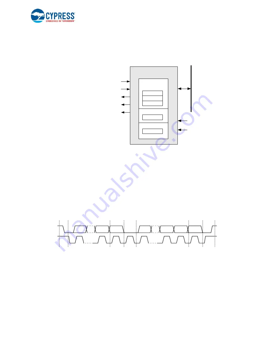
Figure 15-2. I
2
C Slave Block Diagram
enCoRe V
15.1.1
Basic I
2
C Data Transfer
shows the basic form of data transfers on the
I
2
C bus with a 7-bit address format. For a detailed descrip-
tion, see the Philips Semiconductors (now NXP Semicon-
ductors) I
2
C-Bus Specification, version 2.1.
A Start condition (generated by the master) is followed by a
data byte, consisting of a 7-bit slave address (there is also a
10-bit address mode) and a read/write (RW) bit. The RW bit
sets the direction of data transfer. The addressed slave is
required to acknowledge (ACK) the bus by pulling the data
line low during the ninth bit time. If the ACK is received, the
transfer proceeds and the master transmits or receives an
indeterminate number of bytes, depending upon the RW
direction. If, for any reason, the slave does not respond with
an ACK, a Stop condition is generated by the master to ter-
minate the transfer or a Restart condition is generated for a
retry attempt.
Figure 15-3. Basic I
2
C Data Transfer with 7-Bit Address Format
I2C Core
I2C Basic
Configuration
I2C_ CFG
I2C_ SCR
I2C_ DR
Plus Features
HW Addr Cmp
I2C_ ADDR
SDA_OUT
SCL_IN
SYSCLK
I2C_EN
To/From
GPIO
Pins
STANDBY
SCL_OUT
SDA_IN
I2C_XCFG
System B
us
1
7
8
9
1
7
8
9
START
7-Bit Address
R/W
ACK
8-Bit Data
ACK/NACK
STOP


