enCoRe™ V CY7C643xx, enCoRe™ V LV CY7C604xx TRM, Document No. 001-32519 Rev *H
129
SPI
18.3
Timing Diagrams
18.3.1
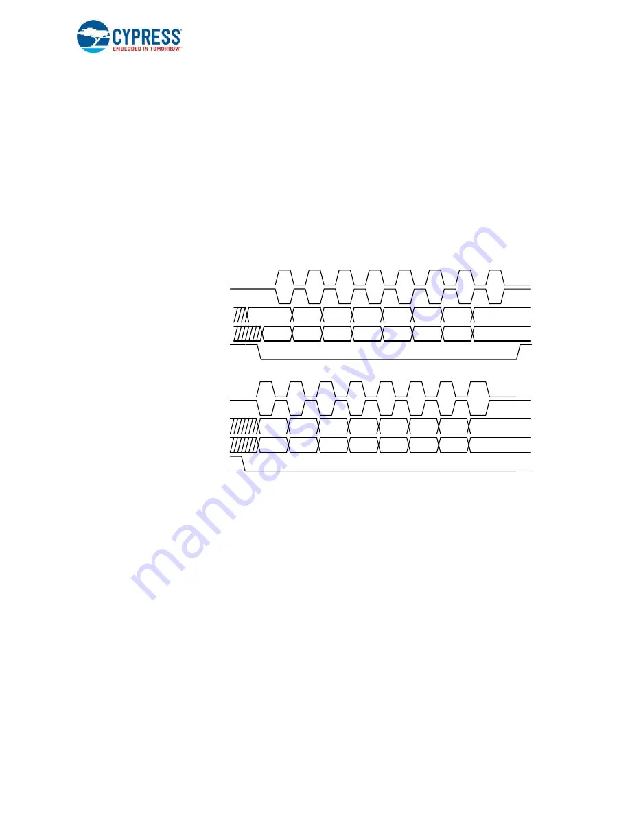
SPI Mode Timing
shows the SPI modes that are typically defined as 0, 1, 2, or 3. These mode numbers are an encoding of two con-
trol bits: Clock Phase and Clock Polarity.
Clock Phase indicates the relationship of the clock to the data. When the clock phase is '0', it means that the data is registered
as an input on the leading edge of the clock and the next data is output on the trailing edge of the clock. When the clock
phase is '1', it means that the next data is output on the leading edge of the clock and that data is registered as an input on the
trailing edge of the clock.
Clock Polarity controls clock inversion. When clock polarity is set to '1’, the clock idle state is high.
Figure 18-3. SPI Mode Timing
MODE 2, 3 (Phase=1)
Output on leading edge. Input on trailing edge.
SCLK, Polarity=0 (Mode 2)
MOSI
MISO
SCLK, Polarity=1 (Mode 3)
7
6
5
4
3
2
1
0
MODE 0, 1 (Phase=0)
Input on leading edge. Output on trailing edge.
SCLK, Polarity=0 (Mode 0)
MOSI
MISO
SCLK, Polarity=1 (Mode 1)
7
6
5
4
3
2
1
0
SS_
SS_