6 F 2 T 0 1 7 2
3.3.3 Trip Circuit Supervision
The circuit breaker tripping control circuit can be monitored by either one or two binary inputs, as
described below.
Trip Circuit Supervision by 1 binary input
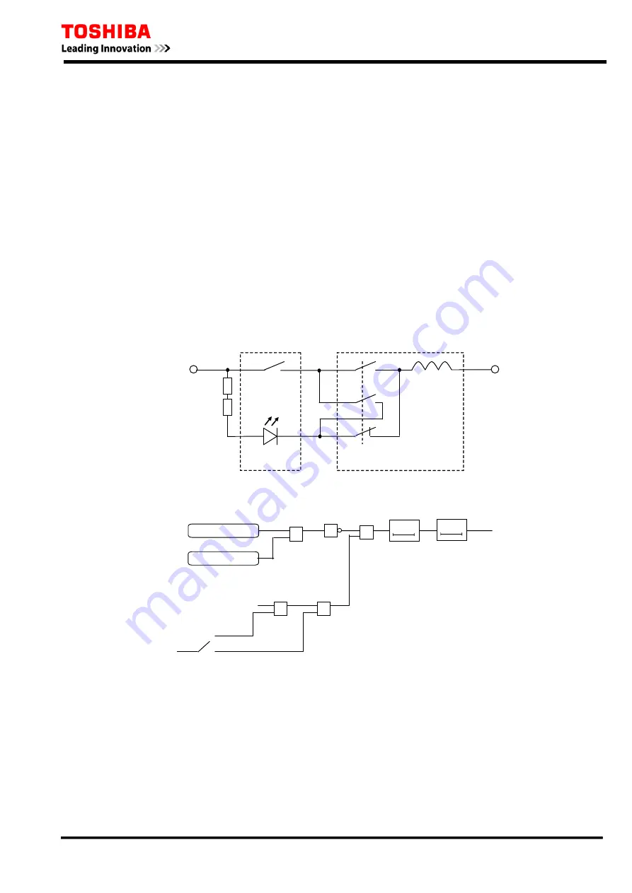
The circuit breaker tripping control circuit can be monitored by one binary input. Figure 3.3.1
shows a typical scheme. When the trip circuit is complete, a small current flows through the binary
input, the circuit breaker auxiliary contacts and the trip coil. This current flows for both the breaker
open and closed conditions. Then logic signal output of the binary input circuit TC FAIL is "1"
under healthy conditions.
If the trip supply is lost or if a connection becomes an open circuit, then the binary input resets and
TC FAIL becomes "0". Figure 3.3.2 shows the scheme logic. A trip circuit fail alarm TCSV is
output when TC FAIL is "0".
The monitoring is enabled by setting the scheme switch [TCSPEN] to "ON" or "OPT-ON" and the
one BI selected "TCFAIL". When "OPT-ON" is selected, the monitoring is enabled only while CB
is closed.
GRE110
Circuit Breaker
Binary
Input
CB Aux.
Contacts
CB Trip Coil
Trip Output
+ve
Trip
Supply
-ve Trip
Supply
Figure 3.3.1 Trip Circuit Supervision by 1 binary input
TC FAIL
1
[TCSPEN]
&
&
+
"ON"
"OPT-ON"
≥
1
CB status “closed”
(BI command)
TCSV
0.4s
t 0
TC FAIL
(BI command)
≥
1
0.4s
0 t
Figure 3.3.2 Supervision Scheme Logic
Trip Circuit Supervision by 2 binary inputs
The circuit breaker tripping control circuit can be monitored by two binary inputs. Figure 3.3.3
shows a typical scheme. When the trip circuit is complete, a small current flows in photo-couplers,
the circuit breaker auxiliary contacts and the trip coil. This current flows for both the breaker open
and closed conditions.
If the trip circuit supply is lost or if a connection becomes open circuit then the TCS issues a Trip
Circuit Fail alarm.
71
Summary of Contents for GRE110
Page 183: ...6 F 2 T 0 1 7 2 Appendix B Signal List 184 ...
Page 191: ...6 F 2 T 0 1 7 2 Appendix C Event Record Items 192 ...
Page 196: ...6 F 2 T 0 1 7 2 Appendix D Binary Output Default Setting List 197 ...
Page 199: ...6 F 2 T 0 1 7 2 Appendix E Relay Menu Tree 200 ...
Page 210: ...6 F 2 T 0 1 7 2 Appendix F Case Outline 211 ...
Page 211: ...6 F 2 T 0 1 7 2 Case Outline for model 400 401 420 421 820 and 821 212 ...
Page 212: ...6 F 2 T 0 1 7 2 Case Outline for model 402 and 422 213 ...
Page 213: ...6 F 2 T 0 1 7 2 Appendix G Typical External Connection 214 ...
Page 245: ...6 F 2 T 0 1 7 2 Appendix J Return Repair Form 246 ...
Page 249: ...6 F 2 T 0 1 7 2 Customer Name Company Name Address Telephone No Facsimile No Signature 250 ...
Page 250: ...6 F 2 T 0 1 7 2 Appendix K Technical Data 251 ...
Page 256: ...6 F 2 T 0 1 7 2 Appendix L Symbols Used in Scheme Logic 257 ...
Page 259: ...6 F 2 T 0 1 7 2 Appendix M Modbus Interoperability 260 ...
Page 289: ...6 F 2 T 0 1 7 2 Appendix N IEC60870 5 103 Interoperability 290 ...
Page 296: ...6 F 2 T 0 1 7 2 Appendix O PLC Default setting 297 ...
Page 298: ...6 F 2 T 0 1 7 2 Appendix P Inverse Time Characteristics 299 ...
Page 304: ...6 F 2 T 0 1 7 2 Appendix Q IEC61850 Interoperability 305 ...


