OfficeServ 7100 Service Manual
© SAMSUNG Electronics Co., Ltd.
2-29
y
Programmable debouncing on one input
y
Time slot assigner
y
Programmable clock slot and PCM transmit clock edge option
2.5.8 8HYB/8COMBO Board
8HYB and 8COMBO boards can use the 8SLI and 8DLI functions and mounted on the
universal slot of OfficeServ 7100.
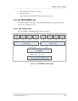
2.5.8.1 Block Diagram-DLI
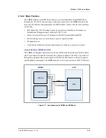
DLI block diagram of 8HYB/8COMBO board is as follows:
Figure 2.15 8HYB/8COMBO DLI Block Diagram
Line #1
Interface
Line #2
Interface
Line #3
Interface
Line #4
Interface
QDASL(TP3404)
Line #5
Interface
Line #6
Interface
Line #7
Interface
Line #8
Interface
QDASL(TP3404)
ASIC(STS9511)
Address & Control
DATA
30 Pin x 2 Connectors(to Mother Board)
Address & Control
DATA
Summary of Contents for OFFICESERV 7100
Page 1: ...Ed 00 OfficeServ 7100 Service Manual ...
Page 33: ...OfficeServ 7100 Service Manual SAMSUNG Electronics Co Ltd 1 15 ...
Page 189: ...OfficeServ 7100 Service Manual SAMSUNG Electronics Co Ltd 5 3 Soldering Side ...
Page 195: ...OfficeServ 7100 Service Manual SAMSUNG Electronics Co Ltd 5 9 5 7 TEPRI2 Board Part Side ...
Page 197: ...OfficeServ 7100 Service Manual SAMSUNG Electronics Co Ltd 5 11 5 8 8COMBO Part Side ...
Page 199: ...OfficeServ 7100 Service Manual SAMSUNG Electronics Co Ltd 5 13 5 9 16DLI2 Part Side ...
Page 201: ...OfficeServ 7100 Service Manual SAMSUNG Electronics Co Ltd 5 15 5 10 MGI16 MGI32 Part Side ...
Page 203: ...OfficeServ 7100 Service Manual SAMSUNG Electronics Co Ltd 5 17 5 11 16SLI2 16MWSLI Part Side ...
Page 205: ...OfficeServ 7100 Service Manual SAMSUNG Electronics Co Ltd 5 19 5 12 8TRK Board Part Side ...
Page 207: ...OfficeServ 7100 Service Manual SAMSUNG Electronics Co Ltd 5 21 5 13 PLIM Board Part Side ...


