CDJ-800MK2
115
5
6
7
8
5
6
7
8
C
D
F
A
B
E
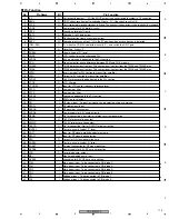
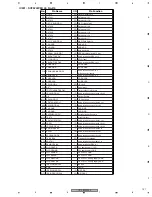
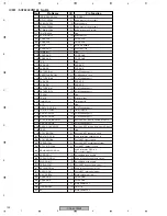
No.
Pin Name
I/O
Pin Function
1
IPF
O
Correction flag output. "H" if the AOUT output is an uncorrectable symbol in C2 correction.
2
SBOK
O
CRCC check result output for subcode Q data. "H" if the check result is OK.
3
CLCK
I/O
Clock input/output for reading subcode P to W data. The polarity of the input/output can be selected with a command.
4
VDD3
−
Power supply for 3.3V digital circuits.
5
VSS3
−
Grounding for digital circuits.
6
DATA
O
Subcode P to W data output.
7
SFSY
O
Playback section frame sync signal output.
8
SBSY
I/O
Subcode block sync output. "H" in the S1 position when a subcode sync is detected.
9
IO0A (RW)
O
"H" when the CD-RW is detected (usually "L"), and switch the OEIC gain.
Unsetting. Always "L"
10
IO1A
O
11
ARSEL
I
Usually fixed at "H" level.
12
AWRC
O
VCO control for active wide-range PLL.
13
PVDD3
−
3.3V power supply dedicated to the PLL section.
14
PDO
O
Signal output for phase difference between EFM and PLCK signals.
15
TMAXS
O
TMAX detection result output. The same signal is output from the TMAX and TMAXS pins.
16
TMAX
O
TMAX detection result output. The same signal is output from the TMAX and TMAXS pins.
17
LPFN
I
Inversion input for PLL section low-pass filter amplifier.
18
LPFO
O
Output for PLL section low-pass filter amplifier.
19
PVREF
−
1.65V reference voltage dedicated to the PLL section.
20
VCOF
O
VCO filter pin.
21
VCOREF
I
Input for VCO center frequency reference level.
22
DTCN
O
Analog slicer filter.
23
DTCP
O
Analog slicer filter.
24
PVSS3
−
Grounding dedicated to the PLL section.
25
SLCO
I
EFM slice level output.
26
RFI
I
RF signal input. An input resistance can be selected using a command.
27
RFRPI
I
RF ripple signal input.
28
RFEQO
O
RF equalizer circuit output.
29
AVDD3
−
Power supply for 3.3V analog circuits.
30
RESIN
I
Pin for connecting a rtesistor for reference current generation.
31
VRO
O
1.65V reference voltage output.
32
VMDIR
−
1.533V reference voltage output.
33
TESTR
O
Pin for connecting filter for RFEQO offset correction.
34
INVSEL
I
Test pin, usually fixed at "L" level.
35
AGCI
I
Input for RF signal amplitude adjustment amp.
36
RFDCI
I
Input for RF signal peak detection.
37
RFO
O
Output for RF signal generation amp.
38
PNSEL
I
Test pin, usually fixed at "H" level.
39
EQSET
O
External-connection for RF signal equalizer.
40
RVDD3
−
Power supply for 3.3V RF amp. core section.
41
LDO
O
Laser diode amp. output.
42
MDI
I
Monitor photodiode amp. input.
43
RVSS3
−
Grounding for 3.3V RF amp. core section.
44
FNI2
I
Main beam input. To be connected to PIN diode C.
45
FNI1
I
Main beam input. To be connected to PIN diode A.
46
FPI2
I
Main beam input. To be connected to PIN diode D.
47
FPI1
I
Main beam input. To be connected to PIN diode B.
48
TPI
I
Subbeam input. To be connected to PIN diode F.
49
FNI
I
Subbeam input. To be connected to PIN diode E.
Pin Function
Summary of Contents for CDJ-800MK2
Page 27: ...CDJ 800MK2 27 5 6 7 8 5 6 7 8 C D F A B E MODE MODE 3 3 A 27 24 26 19 36 ...
Page 29: ...CDJ 800MK2 29 5 6 7 8 5 6 7 8 C D F A B E Data PANEL DATA Digital A 2 3 3 3 A 3 3 A 23 ...
Page 130: ...CDJ 800MK2 130 1 2 3 4 1 2 3 4 C D F A B E Pin Function ...
Page 135: ...CDJ 800MK2 135 5 6 7 8 5 6 7 8 C D F A B E Pin Function ...
Page 139: ...CDJ 800MK2 139 5 6 7 8 5 6 7 8 C D F A B E Pin Function ...
Page 143: ...CDJ 800MK2 143 5 6 7 8 5 6 7 8 C D F A B E ...
Page 153: ...CDJ 800 7 5 6 7 8 5 6 7 8 C D F A B E ...

