background image

186

User’s Manual  U11302EJ4V0UM

CHAPTER 11   BUZZER OUTPUT CONTROLLER

11.1  Buzzer Output Controller Functions

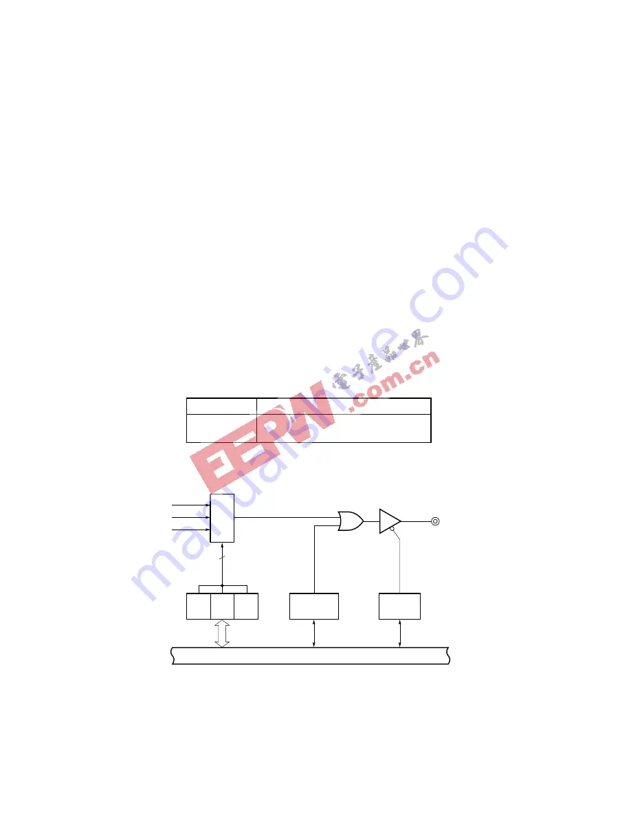
The buzzer output controller outputs a 1.2 kHz, 2.4 kHz, or 4.9 kHz frequency square-wave.  The buzzer

frequency selected by timer clock select register 2 (TCL2) is output from the BUZ/P36 pin.

Follow the procedure below to output the buzzer frequency.

[1] Select the buzzer output frequency using bits 5 to 7 (TCL25 to TCL27) of TCL2.

[2] Set the P36 output latch to 0.

[3] Set bit 6 (PM36) of port mode register 3 (PM3) to 0 (set to output mode).

Caution

Buzzer output cannot be used when the P36 output latch is set to 1.

11.2  Buzzer Output Controller Configuration

The buzzer output controller consists of the following hardware.

Table 11-1.  Buzzer Output Controller Configuration

Item

Configuration

Control registers

Timer clock select register 2 (TCL2)

Port mode register 3 (PM3)

Figure 11-1.  Buzzer Output Controller Block Diagram

f

X

/2

10

f

X

/2

11

f

X

/2

12

P36
output
latch

3

BUZ/P36

PM36

TCL27TCL26TCL25

Internal bus

Timer clock select
register 2

Port mode register 3

Selector

Summary of Contents for mPD780204

Page 1: ...ries 8 Bit Single Chip Microcontrollers µPD780204 µPD780204A µPD780205 µPD780205A µPD780206 µPD780208 µPD78P0208 Document No U11302EJ4V0UM00 4th edition Date Published July 2003 N CP K Printed in Japan User s Manual c ...

Page 2: ...2 User s Manual U11302EJ4V0UM MEMO ...

Page 3: ...luding work bench and floor should be grounded The operator should be grounded using wrist strap Semiconductor devices must not be touched with bare hands Similar precautions need to be taken for PW boards with semiconductor devices on it 2 HANDLING OF UNUSED INPUT PINS FOR CMOS Note No connection for CMOS device inputs can be cause of malfunction If no connection is provided to the input pins it ...

Page 4: ... to persons arising from defects in NEC Electronics products customers must incorporate sufficient safety measures in their design such as redundancy fire containment and anti failure features NEC Electronics products are classified into the following three quality grades Standard Special and Specific The Specific quality grade applies only to NEC Electronics products developed based on a customer...

Page 5: ...nch Seoul Korea Tel 02 558 3737 NEC Electronics Shanghai Ltd Shanghai P R China Tel 021 6841 1138 NEC Electronics Taiwan Ltd Taipei Taiwan Tel 02 2719 2377 NEC Electronics Singapore Pte Ltd Novena Square Singapore Tel 6253 8311 J03 4 NEC Electronics Europe GmbH Duesseldorf Germany Tel 0211 65 03 01 Sucursal en España Madrid Spain Tel 091 504 27 87 Vélizy Villacoublay France Tel 01 30 67 58 00 Succ...

Page 6: ... EVENT COUNTER p 133 Modification of Caution in Figure 6 8 Format of External Interrupt Mode Register p 144 Modification of 6 6 5 Valid edge setting CHAPTER 8 WATCH TIMER p 171 Modification of Caution in Figure 8 2 Format of Timer Clock Select Register 2 CHAPTER 9 WATCHDOG TIMER p 178 Modification of Caution in Figure 9 2 Format of Timer Clock Select Register 2 CHAPTER 11 BUZZER OUTPUT CONTROLLER ...

Page 7: ...is manual in the order of the CONTENTS For how to interpret the register format For a bit number enclosed in angle brackets the bit name is defined as a reserved word in the RA78K0 and is defined in the header file named sfrbit h in the CC78K0 To confirm the details of a register whose register name is known Refer to APPENDIX C REGISTER INDEX For the details of µPD780208 Subseries instruction func...

Page 8: ...ge U11789E CC78K0 C Compiler Operation U14297E Language U14298E SM78K Series System Simulator Ver 2 30 or Later Operation WindowsTM Based U15373E External Part User Open Interface Specification U15802E ID78K Series Integrated Debugger Ver 2 30 or Later Operation Windows Based U15185E RX78K0 Real Time OS Fundamentals U11537E Installation U11536E Project Manager Ver 3 12 or Later Windows Based U1461...

Page 9: ...ducts and Packages X13769X Semiconductor Device Mount Manual Note Quality Grades on NEC Semiconductor Devices C11531E NEC Semiconductor Device Reliability Quality Control System C10983E Guide to Prevent Damage for Semiconductor Devices by Electrostatic Discharge ESD C11892E Note See the Semiconductor Device Mount Manual website http www necel com pkg en mount index html Caution The related documen...

Page 10: ... 1 38 2 2 3 P20 to P27 Port 2 39 2 2 4 P30 to P37 Port 3 39 2 2 5 P70 to P74 Port 7 40 2 2 6 P80 to P87 Port 8 40 2 2 7 P90 to P97 Port 9 40 2 2 8 P100 to P107 Port 10 41 2 2 9 P110 to P117 Port 11 41 2 2 10 P120 to P127 Port 12 41 2 2 11 FIP0 to FIP12 41 2 2 12 VLOAD 42 2 2 13 AVREF 42 2 2 14 AVDD 42 2 2 15 AVSS 42 2 2 16 RESET 42 2 2 17 X1 and X2 42 2 2 18 XT1 and XT2 42 2 2 19 VDD 42 2 2 20 VSS...

Page 11: ...ressing 77 3 4 7 Based addressing 78 3 4 8 Based indexed addressing 79 3 4 9 Stack addressing 79 CHAPTER 4 PORT FUNCTIONS 80 4 1 Port Functions 80 4 2 Port Configuration 83 4 2 1 Port 0 83 4 2 2 Port 1 85 4 2 3 Port 2 86 4 2 4 Port 3 88 4 2 5 Port 7 89 4 2 6 Port 8 90 4 2 7 Port 9 91 4 2 8 Port 10 92 4 2 9 Port 11 93 4 2 10 Port 12 94 4 3 Port Function Control Registers 95 4 4 Port Function Operat...

Page 12: ...eration 140 6 5 5 Square wave output operation 142 6 6 16 Bit Timer Event Counter Operating Precautions 143 CHAPTER 7 8 BIT TIMER EVENT COUNTER 145 7 1 8 Bit Timer Event Counter Functions 145 7 1 1 8 bit timer event counter mode 145 7 1 2 16 bit timer event counter mode 148 7 2 8 Bit Timer Event Counter Configuration 150 7 3 8 Bit Timer Event Counter Control Registers 153 7 4 8 Bit Timer Event Cou...

Page 13: ...nnel 0 207 13 3 Control Registers of Serial Interface Channel 0 211 13 4 Operations of Serial Interface Channel 0 217 13 4 1 Operation stop mode 217 13 4 2 3 wire serial I O mode operation 218 13 4 3 SBI mode operation 223 13 4 4 2 wire serial I O mode operation 249 13 4 5 SCK0 P27 pin output manipulation 255 CHAPTER 14 SERIAL INTERFACE CHANNEL 1 256 14 1 Functions of Serial Interface Channel 1 25...

Page 14: ...vicing Operations 347 16 4 1 Non maskable interrupt request acknowledgment operation 347 16 4 2 Maskable interrupt request acknowledgment operation 350 16 4 3 Software interrupt request acknowledgment operation 352 16 4 4 Multiple interrupt servicing 353 16 4 5 Interrupt request hold 356 16 5 Test Functions 357 16 5 1 Test function control registers 357 16 5 2 Test input signal acknowledgment oper...

Page 15: ...401 B 3 Control Software 402 B 4 PROM Programming Tools 403 B 4 1 Hardware 403 B 4 2 Software 403 B 5 Debugging Tools Hardware 404 B 5 1 When using in circuit emulator IE 78K0 NS IE 78K0 NS A 404 B 5 2 When using in circuit emulator IE 78001 R A 405 B 6 Debugging Tools Software 406 B 7 Embedded Software 407 B 8 Method for Upgrading from Former In Circuit Emulator for 78K 0 Series to IE 78001 R A 4...

Page 16: ...and P04 84 4 3 Block Diagram of P01 to P03 84 4 4 Block Diagram of P10 to P17 85 4 5 Block Diagram of P20 P21 P23 to P26 86 4 6 Block Diagram of P22 and P27 87 4 7 Block Diagram of P30 to P37 88 4 8 Block Diagram of P70 to P74 89 4 9 Block Diagram of P80 to P87 90 4 10 Block Diagram of P90 to P97 91 4 11 Block Diagram of P100 to P107 92 4 12 Block Diagram of P110 to P117 93 4 13 Block Diagram of P...

Page 17: ...cified 140 6 17 External Event Counter Configuration Diagram 141 6 18 External Event Counter Operation Timing with Rising Edge Specified 141 6 19 Square Wave Output Operation Timing 142 6 20 16 Bit Timer Register Start Timing 143 6 21 Timing After Compare Register Change During Timer Count Operation 143 6 22 Capture Register Data Retention Timing 144 7 1 Block Diagram of 8 Bit Timer Event Counter ...

Page 18: ...4 Basic Operation of A D Converter 198 12 5 Relationship Between Analog Input Voltage and A D Conversion Result 199 12 6 A D Conversion by Hardware Start 200 12 7 A D Conversion by Software Start 201 12 8 Example of Method of Reducing Power Consumption in Standby Mode 202 12 9 Analog Input Pin Processing 203 12 10 A D Conversion End Interrupt Request Generation Timing 204 12 11 AVDD Pin Connection...

Page 19: ...atic Data Transmit Receive Interval Specification Register 265 14 6 3 Wire Serial I O Mode Timing 270 14 7 Circuit for Switching Transfer Bit Order 271 14 8 Basic Transmission Reception Mode Operation Timing 279 14 9 Basic Transmission Reception Mode Flowchart 280 14 10 Buffer RAM Operation in 6 Byte Transmission Reception in Basic Transmission Reception Mode 281 14 11 Basic Transmission Mode Oper...

Page 20: ...tputs in 35 Segment x 16 Digit Display Mode 321 15 18 Display Data Memory Configuration and Data Reading Order Display Mode 2 322 15 19 Segment Connection Example 323 15 20 Grid Driving Timing 324 15 21 Data Memory Status in 23 Segment x 5 Grid Display Mode 325 15 22 Allowable Total Power Dissipation PT TA 40 to 85 C 326 15 23 Relationship Between Display Data Memory Contents and Segment Outputs i...

Page 21: ...5 17 5 STOP Mode Release by RESET Input 366 18 1 Block Diagram of Reset Function 367 18 2 Timing of Reset by RESET Input 368 18 3 Timing of Reset due to Watchdog Timer Overflow 368 18 4 Timing of Reset by RESET Input in STOP Mode 368 19 1 Format of Internal Memory Size Switching Register IMS 373 19 2 Format of Internal Expansion RAM Size Switching Register 374 19 3 Page Program Mode Flowchart 377 ...

Page 22: ...mer Event Counter Square Wave Output Ranges 142 7 1 8 Bit Timer Event Counter Interval Time 146 7 2 8 Bit Timer Event Counter Square Wave Output Ranges 147 7 3 Interval Time When 8 Bit Timer Event Counter Is Used as 16 Bit Timer Event Counter 148 7 4 Square Wave Output Ranges When 8 Bit Timer Event Counter Is Used as 16 Bit Timer Event Counter 149 7 5 8 Bit Timer Event Counter Configuration 150 7 ...

Page 23: ...hting Timing 324 16 1 Interrupt Source List 336 16 2 Various Flags Corresponding to Interrupt Request Sources 339 16 3 Times from Maskable Interrupt Request Generation to Interrupt Servicing 350 16 4 Interrupt Request Enabled for Multiple Interrupt During Interrupt Servicing 353 17 1 HALT Mode Operating Status 361 17 2 Operation After HALT Mode Release 363 17 3 STOP Mode Operating Status 364 17 4 ...

Page 24: ...inimum instruction execution time can be changed from high speed 0 4 µs 5 0 MHz operation with main system clock to ultra low speed 122 µs 32 768 kHz operation with subsystem clock 74 I O ports VFD controller driver 53 display outputs in total Segments 9 to 40 Digits 2 to 16 8 bit resolution A D converter 8 channels Power supply voltage AVDD 4 0 to 5 5 V Serial interface 2 channels 3 wire serial I...

Page 25: ...FP 14 x 20 Mask ROM µPD780208GF xxx 3BA 100 pin plastic QFP 14 x 20 Mask ROM µPD78P0208GF 3BA 100 pin plastic QFP 14 x 20 One time PROM Remark xxx indicates ROM code suffix 1 4 Quality Grade Part Number Package Quality Grade µPD780204GF xxx 3BA 100 pin plastic QFP 14 x 20 Standard µPD780204AGF xxx 3BA 100 pin plastic QFP 14 x 20 Standard µPD780205GF xxx 3BA 100 pin plastic QFP 14 x 20 Standard µPD...

Page 26: ...TI1 P32 TO2 P31 TO1 P30 TO0 RESET X2 X1 IC VPP XT2 P04 XT1 VDD P27 SCK0 P26 SO0 SB1 P25 SI0 SB0 P24 BUSY P23 STB P22 SCK1 P21 SO1 P20 SI1 AVSS P17 ANI7 P16 ANI6 P15 ANI5 P14 ANI4 P13 ANI3 1 2 3 4 5 6 7 8 9 10 11 12 13 14 15 16 17 18 19 20 21 22 23 24 25 26 27 28 29 30 80 79 78 77 76 75 74 73 72 71 70 69 68 67 66 65 64 63 62 61 60 59 58 57 56 55 54 53 52 51 P87 FIP20 VLOAD P90 FIP21 P91 FIP22 P92 F...

Page 27: ...ve power supply VPP Programming power supply VSS Ground X1 X2 Crystal main system clock XT1 XT2 Crystal subsystem clock ANI0 to ANI7 Analog input AVDD Analog power supply AVREF Analog reference voltage AVSS Analog ground BUSY Busy BUZ Buzzer clock FIP0 to FIP52 Fluorescent indicator panel IC Internally connected INTP0 to INTP3 External interrupt input P00 to P04 Port 0 P10 to P17 Port 1 P20 to P27...

Page 28: ...ble PGM Program VPP Programming power supply D0 to D7 Data bus RESET Reset VSS Ground VDD D7 D6 D5 D4 D3 D2 D1 D0 RESET Open L VPP Open L VDD A7 A6 A5 A4 A3 A2 A1 A0 VSS CE OE L D L D D 1 2 3 4 5 6 7 8 9 10 11 12 13 14 15 16 17 18 19 20 21 22 23 24 25 26 27 28 29 30 80 79 78 77 76 75 74 73 72 71 70 69 68 67 66 65 64 63 62 61 60 59 58 57 56 55 54 53 52 51 L VSS A8 A16 A10 A11 A12 A13 A14 A15 L L D ...

Page 29: ...ubseries products are compatible with I2 C bus ROMless version of the PD78078 µ 100 pin µ µ 100 pin EMI noise reduced version of the PD78078 µ Inverter control PD780208 100 pin VFD drive PD78044F with enhanced I O and VFD C D Display output total 53 µ µ PD78098B µ 100 pin PD780024A PD780024AY µ µ µ 80 pin 80 pin PD780852 PD780828B µ µ For automobile meter driver On chip CAN controller 100 pin PD78...

Page 30: ... ch 3 ch UART 2 ch 47 4 0 V control VFD PD780208 32 K to 60 K 2 ch 1 ch 1 ch 1 ch 8 ch 2 ch 74 2 7 V drive PD780232 16 K to 24 K 3 ch 4 ch 40 4 5 V PD78044H 32 K to 48 K 2 ch 1 ch 1 ch 8 ch 1 ch 68 2 7 V PD78044F 16 K to 40 K 2 ch LCD PD780354 24 K to 32 K 4 ch 1 ch 1 ch 1 ch 8 ch 3 ch UART 1 ch 66 1 8 V drive PD780344 8 ch PD780338 48 K to 60 K 3 ch 2 ch 10 ch 1 ch 2 ch UART 1 ch 54 PD780328 62 P...

Page 31: ...terrupt control Clock output control Buzzer output TO0 P30 TI0 P00 TO1 P31 TI1 P33 TO2 P32 TI2 P34 SI0 SB0 P25 SO0 SB1 P26 SCK0 P27 SI1 P20 SO1 P21 SCK1 P22 STB P23 BUSY P24 ANI0 P10 to ANI7 P17 AVDD AVSS AVREF INTP0 P00 to INTP3 P03 BUZ P36 PCL P35 78K 0 CPU core ROM RAM VDD VSS IC VPP Port 0 Port 1 Port 2 Port 3 Port 7 Port 8 Port 9 Port 10 Port 11 Port 12 VFD controller driver System control P0...

Page 32: ...6 pins VFD controller driver Total of display output 53 pins Segments 9 to 40 pins Digits 2 to 16 pins A D converter 8 bit resolution x 8 channels Power supply voltage AVDD 4 0 to 5 5 V Serial interface 3 wire serial I O SBI 2 wire serial I O mode selection possible 1 channel 3 wire serial I O mode maximum 64 byte on chip automatic transmit receive function 1 channel Notes 1 The initial value of t...

Page 33: ...tors and pull down resistors listed in Table 1 1 can be incorporated When these resistors are necessary the number of external components and mounting space can be saved by utilizing the mask options Table 1 1 shows the mask options provided in the µPD780208 Subseries products Table 1 1 Mask Options in Mask ROM Versions Pin Name Mask Option P30 TO0 to P32 TO2 P33 TI1 P34 TI2 On chip pull down resi...

Page 34: ...essor clock control register PCC to 1 do not use the feedback resistor contained in the subsystem clock oscillator 2 When the P10 ANI0 to P17 ANI7 pins are used as analog inputs of the A D converter set port 1 to the input mode In this case its on chip pull up resistor will be automatically disabled Port 0 5 bit I O port Input output can be specified in 1 bit units If used as an input port use of ...

Page 35: ...e mask option connection to VLOAD or VSS is specifiable in 4 bit units P100 to P107 I O Port 10 Input FIP29 to FIP36 P ch open drain 8 bit high withstanding voltage I O port Input output can be specified in 1 bit units LEDs can be driven directly In mask ROM versions use of an on chip pull down resistor can be specified in 1 bit units with the mask option connection to VLOAD or VSS is specifiable ...

Page 36: ...ock output for trimming main system clock and subsystem clock Input P35 BUZ Output Buzzer output Input P36 FIP0 to FIP12 Output High withstanding voltage and high current output for VFD controller Output driver display output In mask ROM versions use of an on chip pull down resistor can be specified with the mask option The µPD78P0208 has on chip pull down resistors connected to VLOAD FIP13 to FIP...

Page 37: ...ntial IC Internally connected Connect directly to VSS 2 1 2 PROM programming mode pins µPD78P0208 only Pin Name I O Function RESET Input PROM programming mode setting When 5 V or 12 5 V is applied to the VPP pin or a low level voltage is applied to the RESET pin the PROM programming mode is set VPP Input High voltage application for PROM programming mode setting and program write verify A0 to A16 ...

Page 38: ...3 INTP0 to INTP2 are external interrupt request input pins for which valid edges can be specified rising edge falling edge and both rising and falling edges INTP0 becomes a 16 bit timer event counter capture trigger signal input pin with a valid edge input INTP3 becomes a falling edge detection external interrupt request input pin b TI0 TI0 is a pin for inputting the external count clock to the 16...

Page 39: ...NEC Electronics standard serial bus interface I O pins d BUSY Serial interface automatic transmit receive busy input pin e STB Serial interface automatic transmit receive strobe output pin Caution If port 2 is used as serial interface pins the I O and output latches must be set according to the function For the setting method refer to Figure 13 3 Format of Serial Operating Mode Register 0 and Figu...

Page 40: ...FD controller driver Port 8 can drive LEDs directly The following operating modes can be specified in 1 bit units 1 Port mode P80 to P87 function as an 8 bit output only port P80 to P87 are P ch open drain outputs In mask ROM versions use of pull down resistors can be specified with the mask option 2 Control mode P80 to P87 function as the display output pins of the VFD controller driver FIP13 to ...

Page 41: ...n input or output mode in 1 bit units using port mode register 11 PM11 P110 to P117 are P ch open drain outputs In mask ROM versions use of pull down resistors can be specified with the mask option 2 Control mode P110 to P117 function as display output pins for the VFD controller driver FIP37 to FIP44 2 2 10 P120 to P127 Port 12 These pins constitute an 8 bit I O port Besides serving as I O port p...

Page 42: ...tor connection pins for subsystem clock oscillation For external clock supply input the clock to XT1 and its inverted signal to XT2 2 2 19 VDD This is the positive power supply pin 2 2 20 VSS This is the ground potential pin 2 2 21 VPP µPD78P0208 only A high voltage should be applied to this pin during PROM programming mode setting and in program write verify mode Connect directly to VSS in normal...

Page 43: ...Connect to VSS P01 INTP1 8 A I O Input Independently connect to VSS via a resistor P02 INTP2 Output Leave open P03 INTP3 P04 XT1 16 Input Connect to VDD or VSS P10 ANI0 to P17 ANI7 11 I O Input Independently connect to VDD or VSS via a resistor P20 SI1 8 A Output Leave open P21 SO1 5 A P22 SCK1 8 A P23 STB 5 A P24 BUSY 8 A P25 SI0 SB0 10 A P26 SO0 SB1 P27 SCK0 Mask ROM version P30 TO0 5 C I O Inpu...

Page 44: ...Independently connect to VDD or VSS via a resistorNote P110 FIP37 to P117 FIP44 Output Leave open P120 FIP45 to P127 FIP52 IC Connect directly to VSS µPD78P0208 P70 to P74 13 D I O Input Independently connect to VDD or VSS via a resistor Output Leave open FIP0 to FIP12 14 Output Leave open P80 FIP13 to P87 FIP20 14 B Output Leave open P90 FIP21 to P97 FIP28 P100 FIP29 to P107 FIP36 15 B I O Input ...

Page 45: ... triggered input with hysteresis characteristics Type 5 C Type 10 A Type 8 B Type 8 A Pull up enable VDD P ch IN OUT Output disable Data VDD P ch N ch Pull up enable VDD P ch IN OUT Output disable Data VDD P ch N ch Pull up enable VDD P ch IN OUT Output disable Data VDD P ch N ch Mask option Input enable Pull up enable VDD P ch IN OUT Open drain Output disable Data VDD P ch N ch Mask option ...

Page 46: ...put disable Data VDD P ch N ch P ch Comparator N ch Input enable VREF Threshold voltage VDD P ch N ch VDD P ch Data OUT VLOAD VDD P ch N ch VDD P ch Data OUT VLOAD Mask option Mask option VDD P ch N ch VDD P ch Data OUT Data VDD N ch P ch IN OUT VDD Output disable RD Mask option Middle voltage input buffer Data Output disable IN OUT N ch P ch VDD RD Middle voltage input buffer ...

Page 47: ...er s Manual U11302EJ4V0UM Figure 2 1 Pin I O Circuits 3 3 Type 15 B Type 15 C Type 16 P ch XT2 XT1 Feedback cut off VDD P ch N ch VDD P ch Data IN OUT VLOAD Mask option Mask option RD N ch VDD P ch N ch VDD P ch Data IN OUT RD N ch ...

Page 48: ...use µPD780204A C8H µPD780205A CAH µPD78P0208 Value corresponding to mask ROM version Figure 3 1 Memory Map µPD780204 and µPD780204A 0000H Data memory space Internal ROM 32768 x 8 bits 7FFFH 1000H 0FFFH 0800H 07FFH 0080H 007FH 0040H 003FH 0000H CALLF entry area CALLT table area Program area Program area Internal high speed RAM 1024 x 8 bits Reserved Reserved Program memory space 8000H 7FFFH FFFFH G...

Page 49: ...H 0040H 003FH 0000H CALLF entry area CALLT table area Program area Program area Internal high speed RAM 1024 x 8 bits Reserved Reserved Program memory space A000H 9FFFH FFFFH General purpose registers 32 x 8 bits Special function registers SFRs 256 x 8 bits Vector table area FA30H FA2FH VFD display RAM 80 x 8 bits FA80H FA7FH FAC0H FABFH Buffer RAM 64 x 8 bits FB00H FAFFH FEE0H FEDFH FF00H FEFFH ...

Page 50: ...bits Buffer RAM 64 x 8 bits Reserved VFD display RAM 80 x 8 bits Reserved Internal expansion RAM 1024 x 8 bits Reserved Internal ROM 49152 x 8 bits Program area CALLF entry area Program area CALLT table area Vector table area Program memory space 0000H 0040H 003FH 0080H 007FH 0800H 07FFH 1000H 0FFFH BFFFH FFFFH FF00H FEFFH FEE0H FEDFH FB00H FAFFH FAC0H FABFH FA80H FA7FH FA30H FA2FH F800H F7FFH F40...

Page 51: ...bits Buffer RAM 64 x 8 bits Reserved VFD display RAM 80 x 8 bits Reserved Internal expansion RAM 1024 x 8 bits Reserved Internal ROM 61440 x 8 bits Program area CALLF entry area Program area CALLT table area Vector table area Program memory space FFFFH FF00H FEFFH FEE0H FEDFH FB00H FAFFH FAC0H FABFH FA80H FA7FH FA30H FA2FH F800H F7FFH F400H F3FFH F000H EFFFH 0000H 0000H 0040H 003FH 0080H 007FH 080...

Page 52: ...T table area Program area Program area Internal high speed RAM 1024 x 8 bits Reserved Reserved Program memory space F000H EFFFH FFFFH General purpose registers 32 x 8 bits Special function registers SFRs 256 x 8 bits Vector table area FA30H FA2FH VFD display RAM 80 x 8 bits FA80H FA7FH FAC0H FABFH Buffer RAM 64 x 8 bits FB00H FAFFH FEE0H FEDFH FF00H FEFFH Internal expansion RAM 1024 x 8 bits F800H...

Page 53: ...ed at even addresses and the higher 8 bits are stored at odd addresses Table 3 2 Vector Table Vector Table Address Interrupt Source Vector Table Address Interrupt Source 0000H RESET input 0010H INTCSI1 0004H INTWDT 0012H INTTM3 0006H INTP0 0014H INTTM0 0008H INTP1 0016H INTTM1 000AH INTP2 0018H INTTM2 000CH INTP3 001AH INTAD 000EH INTCSI0 001CH INTKS 003EH BRK instruction 2 CALLT instruction table...

Page 54: ...ta area similar to the internal high speed RAM as well as a program area in which instructions can be written and executed The internal expansion RAM cannot be used as a stack memory 3 Buffer RAM Buffer RAM is allocated to the 64 byte area from FAC0H to FAFFH Buffer RAM is used for storing transmit receive data of serial interface channel 1 3 wire serial I O mode with automatic transmit receive fu...

Page 55: ... is assigned addresses FB00H to FFFFH the special function registers SFRs and general purpose registers can be addressed in accordance with thier function Data memory addressing is shown in Figures 3 6 to 3 10 For details of each addressing refer to 3 4 Operand Address Addressing Figure 3 6 Data Memory Addressing µPD780204 and µPD780204A 0000H Internal ROM 32768 x 8 bits Internal high speed RAM 10...

Page 56: ...64 x 8 bits Reserved A000H 9FFFH FFFFH General purpose registers 32 x 8 bits Special function registers SFRs 256 x 8 bits FB00H FAFFH FAC0H FABFH FEE0H FEDFH FF00H FEFFH VFD display RAM 80 x 8 bits FA80H FA7FH FA30H FA2FH Reserved FF20H FF1FH Direct addressing Register indirect addressing Based addressing Based indexed addressing FE20H FE1FH SFR addressing Register addressing Short direct addressi...

Page 57: ...r RAM 64 x 8 bits Reserved VFD display RAM 80 x 8 bits Reserved Internal expansion RAM 1024 x 8 bits Reserved Internal ROM 49152 x 8 bits SFR addressing Register addressing Short direct addressing Direct addressing Register indirect addressing Based addressing Based indexed addressing FFFFH FF20H FF1FH FF00H FEFFH FEE0H FEDFH FE20H FE1FH FB00H FAFFH FAC0H FABFH FA80H FA7FH FA30H FA2FH F800H F7FFH ...

Page 58: ...r RAM 64 x 8 bits Reserved VFD display RAM 80 x 8 bits Reserved Internal expansion RAM 1024 x 8 bits Reserved Internal ROM 61440 x 8 bits SFR addressing Register addressing Short direct addressing Direct addressing Register indirect addressing Based addressing Based indexed addressing FFFFH FF20H FF1FH FF00H FEFFH FEE0H FEDFH FE20H FE1FH FB00H FAFFH FAC0H FABFH FA80H FA7FH FA30H FA2FH F800H F7FFH ...

Page 59: ...neral purpose registers 32 x 8 bits Special function registers SFRs 256 x 8 bits FB00H FAFFH FA30H FA2FH FEE0H FEDFH FF00H FEFFH Internal expansion RAM 1024 x 8 bits F800H F7FFH F400H F3FFH Reserved FF20H FF1FH Direct addressing Register indirect addressing Based addressing Based indexed addressing FE20H FE1FH SFR addressing Register addressing Short direct addressing FA80H FA7FH FAC0H FABFH VFD d...

Page 60: ...generation or PUSH PSW instruction execution and are automatically reset upon execution of the RETB RETI and POP PSW instructions RESET input sets the PSW to 02H Figure 3 12 Program Status Word Format a Interrupt enable flag IE This flag controls interrupt request acknowledgment operations of the CPU When IE 0 the IE flag is set to the interrupt disabled DI status All interrupts except non maskabl...

Page 61: ...E f Carry flag CY This flag stores overflow and underflow upon add subtract instruction execution It stores the shift out value upon rotate instruction execution and functions as a bit accumulator during bit manipulation instruction execution 3 Stack pointer SP This is a 16 bit register used to hold the start address of the memory stack area Only the internal high speed RAM area FB00H to FEFFH can...

Page 62: ... instructions PUSH rp instruction Lower register pairs Higher register pairs SP SP 2 SP 2 SP 1 SP SP SP 2 SP 2 SP 1 SP PC7 to PC0 PC15 to PC8 SP SP 3 SP 3 SP 2 SP 1 PC15 to PC8 PSW SP PC7 to PC0 RETI and RETB instructions PC15 to PC8 PSW PC7 to PC0 SP SP 3 SP SP 1 SP 2 PC15 to PC8 PC7 to PC0 SP SP 2 SP SP 1 Lower register pairs SP SP 2 SP SP 1 Higher register pairs RET instruction POP rp instructi...

Page 63: ... and HL and absolute names R0 to R7 and RP0 to RP3 Register banks to be used for instruction execution are set using the CPU control instruction SEL RBn Because of the 4 register bank configuration an efficient program can be created by switching between a register for normal processing and a register for interrupts for each bank Figure 3 16 General Purpose Register Configuration a Absolute name b...

Page 64: ...assembler for the 8 bit manipulation instruction operand sfr This manipulation can also be specified with an address 16 bit manipulation Describe the symbol reserved in the assembler for the 16 bit manipulation instruction operand sfrp When addressing an address describe an even address Table 3 3 gives a list of special function registers The meaning of items in the table is as follows Symbol Indi...

Page 65: ...S TM2 FF1AH Serial I O shift register 0 SIO0 R W Undefined FF1BH Serial I O shift register 1 SIO1 FF1FH A D conversion result register ADCR R FF20H Port mode register 0 PM0 R W 1FH FF21H Port mode register 1 PM1 FFH FF22H Port mode register 2 PM2 FF23H Port mode register 3 PM3 FF27H Port mode register 7 PM7 1FH FF2AH Port mode register 10 PM10 FFH FF2BH Port mode register 11 PM11 FF2CH Port mode r...

Page 66: ...ss pointer ADTP FF6BH Automatic data transmit receive interval specification ADTI register FF80H A D converter mode register ADM 01H FF84H A D converter input select register ADIS 00H FFA0H Display mode register 0 DSPM0 Note FFA1H Display mode register 1 DSPM1 FFA2H Display mode register 2 DSPM2 FFE0H Interrupt request flag register 0L xxxx IF0L FFE1H Interrupt request flag register 0H xxxx IF0H F...

Page 67: ... control register PCC Note The value after resetting the internal memory size switching register IMS and internal expansion RAM size switching register IXS depends on the product µPD780204 µPD780204A µPD780205 µPD780205A µPD780206 µPD780208 µPD78P0208 IMS C8H CFH CAH CFH CCH CFH CFH IXS None 0AH When using the µPD780204 780205 780206 and 780208 do not set any value other than that of IMS and IXS a...

Page 68: ...326E 3 3 1 Relative addressing Function The value obtained by adding 8 bit immediate data displacement value jdisp8 of an instruction code to the start address of the following instruction is transferred to the program counter PC and branched The displacement value is treated as signed two s complement data 128 to 127 and bit 7 becomes a sign bit In other words the range of branch in relative addr...

Page 69: ...n the CALL addr16 or BR addr16 or CALLF addr11 instruction is executed CALL addr16 and BR addr16 instructions can branch to all the memory spaces CALLF addr11 instruction branches to the area from 0800H to 0FFFH Illustration In the case of CALL addr16 and BR addr16 instructions In the case of CALLF addr11 instruction 15 0 PC 8 7 7 0 CALL or BR Low addr High addr 15 0 PC 8 7 7 0 fa10 8 11 10 0 0 0 ...

Page 70: ...n code are transferred to the program counter PC and branched Table indirect addressing is carried out when the CALLT addr5 instruction is executed This instruction can refer to the address stored in the memory table 40H to 7FH and branch to all the memory spaces Illustration 15 1 15 0 PC 7 0 Low addr High addr Memory table Effective address 1 Effective address 0 1 0 0 0 0 0 0 0 0 8 7 8 7 6 5 0 0 ...

Page 71: ...3 4 Register addressing Function Register pair AX contents to be specified with an instruction word are transferred to the program counter PC and branched This function is carried out when the BR AX instruction is executed Illustration 7 0 rp 0 7 A X 15 0 PC 8 7 ...

Page 72: ...Instruction Register to Be Specified by Implied Addressing MULU Register A for multiplicand and register AX for product storage DIVUW Register AX for dividend and quotient storage ADJBA ADJBS Register A for storage of numeric values subject to decimal adjustment ROR4 ROL4 Register A for storage of digit data which undergoes digit rotation Operand format Because implied addressing can be automatica...

Page 73: ...the following operand format is executed When an 8 bit register is specified one of the eight registers is specified with 3 bits in the operation code Operand format Identifier Description r X A C B E D L H rp AX BC DE HL r and rp can be described using function names X A C B E D L H AX BC DE and HL as well as absolute names R0 to R7 and RP0 to RP3 Description example MOV A C when selecting C regi...

Page 74: ...e data in an instruction word is directly addressed Operand format Identifier Description addr16 Label or 16 bit immediate data Description example MOV A 0FE00H when setting addr16 to FE00H Illustration Operation code 1 0 0 0 1 1 1 0 0 0 0 0 0 0 0 0 1 1 1 1 1 1 1 0 Opcode 00H FEH 7 0 addr16 lower Opcode Memory addr16 lower ...

Page 75: ...ers of the timer event counter are mapped and these SFRs can be manipulated with a small number of bytes and clocks When 8 bit immediate data is at 20H to FFH bit 8 of an effective address is set to 0 When it is at 00H to 1FH bit 8 is set to 1 Refer to Illustration below Operand format Identifier Description saddr Label or immediate data indicating FE20H to FF1FH saddrp Label or immediate data ind...

Page 76: ...H to FFCFH and FFE0H to FFFFH However the SFRs mapped at FF00H to FF1FH can be accessed with short direct addressing Operand format Identifier Description sfr Special function register name sfrp 16 bit manipulatable special function register name even address only Description example MOV PM0 A when selecting PM0 FF20H as sfr Illustration Operation code 1 1 1 1 0 1 1 0 0 0 1 0 0 0 0 0 15 0 7 0 Opco...

Page 77: ... register bank select flag RBS0 and RBS1 and the register pair specification code in the instruction code This addressing can be carried out for all the memory spaces Operand format Identifier Description DE HL Description example MOV A DE when selecting DE as register pair Illustration Operation code 1 0 0 0 0 1 0 1 15 0 7 8 DE 7 0 A 0 7 D E The contents of addressed memory are transferred Memory...

Page 78: ...ster pair to be accessed is in the register bank specified with the register bank select flags RBS0 and RBS1 Addition is performed by expanding the offset data as a positive number to 16 bits A carry from the 16th bit is ignored This addressing can be carried out for all the memory spaces Operand format Identifier Description HL byte Description example MOV A HL 10H When setting byte to 10H Operat...

Page 79: ...bits A carry from the 16th bit is ignored This addressing can be carried out for all the memory spaces Operand format Identifier Description HL B HL C Description example In the case of MOV A HL B select B register 3 4 9 Stack addressing Function The stack area is indirectly addressed with the stack pointer SP contents This addressing method is automatically employed when the PUSH POP subroutine c...

Page 80: ...s the port configuration Every port is capable of 1 bit and 8 bit manipulations and can carry out various control operations Besides port functions the ports can also serve as on chip hardware I O pins Figure 4 1 Port Types Port 9 P90 P97 P100 P107 P110 P117 P120 P127 P04 P10 P17 P20 P27 P30 P37 P70 P74 P00 P80 P87 Port 10 Port 11 Port 12 Port 1 Port 0 Port 2 Port 3 Port 7 Port 8 ...

Page 81: ...en directly In mask ROM versions use of pull down resistors can be specified in 1 bit units with the mask option can be specified as connected to VLOAD or VSS in 4 bit units P90 to P97 Port 9 FIP21 to FIP28 P ch open drain 8 bit high withstanding voltage output port LEDs can be driven directly In mask ROM versions use of pull down resistors can be specified in 1 bit units with the mask option can ...

Page 82: ...10 to P117 Port 11 FIP37 to FIP44 P ch open drain 8 bit high withstanding voltage I O port Input output can be specified in 1 bit units LEDs can be driven directly In mask ROM versions use of pull down resistors can be specified in 1 bit units with the mask option can be specified as connected to VLOAD or VSS in 4 bit units P120 to P127 Port 12 FIP45 to FIP52 P ch open drain 8 bit high withstandin...

Page 83: ...input mode output mode in 1 bit units using port mode register 0 PM0 The P00 and P04 pins are input only port pins When the P01 to P03 pins are used as input port pins on chip pull up resistors can be connected to them in 3 bit units using the pull up resistor option register PUO Alternate functions include external interrupt request input external count clock input to the timer and crystal connec...

Page 84: ...ure 4 3 Block Diagram of P01 to P03 PUO Pull up resistor option register PM Port mode register RD Port 0 read signal WR Port 0 write signal P00 INTP0 TI0 P04 XT1 RD Internal bus P ch WRPM WRPORT RD WRPUO VDD P01 INTP1 P02 INTP2 P03 INTP3 Selector PUO0 Output latch P01 to P03 PM01 to PM03 Internal bus ...

Page 85: ...nits using the pull up resistor option register PUO Alternate functions include A D converter analog input RESET input sets port 1 to input mode Figure 4 4 shows a block diagram of port 1 Caution A pull up resistor cannot be connected to pins used for A D converter analog input Figure 4 4 Block Diagram of P10 to P17 PUO Pull up resistor option register PM Port mode register RD Port 1 read signal W...

Page 86: ...w block diagrams of port 2 Cautions 1 If used as serial interface pins set the I O and output latch according to each function Refer to Figure 13 3 Format of Serial Operating Mode Register 0 and Figure 14 3 Format of Serial Operating Mode Register 1 for the settings 2 When reading the pin state in SBI mode set the PM2n bit of PM2 to 1 n 5 6 refer to the description of 10 Judging busy status of sla...

Page 87: ...e 4 6 Block Diagram of P22 and P27 PUO Pull up resistor option register PM Port mode register RD Port 2 read signal WR Port 2 write signal P ch WRPM WRPORT RD WRPUO VDD P22 SCK1 P27 SCK0 Selector PUO2 Output latch P22 P27 PM22 PM27 Alternate function Internal bus ...

Page 88: ... 1 bit units with the mask option The µPD78P0208 does not contain pull down resistors Port 3 can drive LEDs directly Alternate functions include timer I O clock output and buzzer output RESET input sets port 3 to input mode Figure 4 7 shows a block diagram of port 3 Figure 4 7 Block Diagram of P30 to P37 PUO Pull up resistor option register PM Port mode register RD Port 3 read signal WR Port 3 wri...

Page 89: ...ries depending on the following conditions For mask ROM version When a pull up resistor is connected 3 µA max regardless of operational conditions When a pull up resistor is not connected 200 µA max during 1 5 clock cycles after read instruction execution to port 7 P7 or port mode register 7 PM7 3 µA max under other conditions For PROM version 200 µA max during 1 5 clock cycles after read instruct...

Page 90: ...s directly Alternate functions include VFD controller driver display output RESET input sets port 8 to output mode Figure 4 9 shows a block diagram of port 8 Caution Adjust the number of pull down resistors so that the total power dissipation refer to 15 10 Calculating Total Power Dissipation is not exceeded Figure 4 9 Block Diagram of P80 to P87 WR Port 8 write signal Internal bus Output latch P8...

Page 91: ... directly Alternate functions include VFD controller driver display output RESET input sets port 9 to output mode Figure 4 10 shows a block diagram of port 9 Caution Adjust the number of pull down resistors so that the total power dissipation refer to 15 10 Calculating Total Power Dissipation is not exceeded Figure 4 10 Block Diagram of P90 to P97 WR Port 9 write signal Internal bus Output latch P...

Page 92: ...tors Port 10 can drive LEDs directly Alternate functions include VFD controller driver display output RESET input sets port 10 to input mode Figure 4 11 shows a block diagram of port 10 Caution Adjust the number of pull down resistors so that the total power dissipation refer to 15 10 Calculating Total Power Dissipation is not exceeded Figure 4 11 Block Diagram of P100 to P107 RD WRPORT Internal b...

Page 93: ...tors Port 11 can drive LEDs directly Alternate functions include VFD controller driver display output RESET input sets port 11 to input mode Figure 4 12 shows a block diagram of port 11 Caution Adjust the number of pull down resistors so that the total power dissipation refer to 15 10 Calculating Total Power Dissipation is not exceeded Figure 4 12 Block Diagram of P110 to P117 PM Port mode registe...

Page 94: ...stors Port 12 can drive LEDs directly Alternate functions include VFD controller driver display output RESET input sets port 12 to input mode Figure 4 13 shows a block diagram of port 12 Caution Adjust the number of pull down resistors so that the total power dissipation refer to 15 10 Calculating Total Power Dissipation is not exceeded Figure 4 13 Block Diagram of P120 to P127 PM Port mode regist...

Page 95: ...d therefore the interrupt mask flag should be set to 1 beforehand Table 4 3 Port Mode Register and Output Latch Setting When Alternate Function Is Used Pin Name Alternate Function PMxx Pxx Pin Name Alternate Function PMxx Pxx P00 INTP0 Input 1 fixed None P33 P34 TI1 TI2 Input 1 X TI0 Input 1 fixed None P35 PCL Output 0 0 P01 P02 INTP1 INTP2 Input 1 X P36 BUZ Output 0 0 P03 INTP3 Input 1 X P100 to ...

Page 96: ...M21 PM36 PM35 PM34 PM33 PM32 PM31 PM17 PM10 PM27 PM3 PM20 PM30 PM12 PMmn Pmn pin I O mode selection m 0 1 2 3 7 10 11 12 n 0 to 7 0 1 Output mode output buffer on Input mode output buffer off FF20H FF2CH FF21H FF22H FF23H 1FH FFH FFH FFH FFH R W R W R W R W R W Address After reset R W 0 PM72 PM71 0 0 PM74 PM73 PM70 PM7 FF27H 1FH R W PM117 PM116 PM115 PM114 PM113 PM112 PM111 PM110 PM11 FF2BH FFH R ...

Page 97: ...rs cannot be used regardless of the PUO register setting PUO is set with a 1 bit or 8 bit memory manipulation instruction RESET input sets this register to 00H Cautions 1 The P00 and P04 pins do not incorporate a pull up resistor 2 When port 1 is used as analog input for the A D converter an on chip pull up resistor cannot be used even if 1 is set in PUO1 Figure 4 15 Format of Pull up Resistor Opt...

Page 98: ... pins the output latch contents for pins specified as input are undefined except for the manipulated bit 4 4 2 Reading from I O port 1 Output mode The output latch contents are read by a transfer instruction The output latch contents do not change 2 Input mode The pin status is read by a transfer instruction The output latch contents do not change 4 4 3 Operations on I O port 1 Output mode An oper...

Page 99: ...rs in 1 bit units Can incorporate pull down resistors in 1 bit units Can incorporate pull down resistors in 1 bit units The pull down resistors can be specified to be connected to VLOAD or VSS in 4 bit units from P80 Does not incorporate pull down resistors Does not incorporate pull up resistors Incorporates pull down resistors connected to VLOAD Does not incorporate pull down resistors P30 TO0 to...

Page 100: ...llates at a frequency of 32 768 kHz Oscillation cannot be stopped If the subsystem clock oscillator is not used the internal feedback resistor can be disabled by the processor clock control register PCC This decreases the power consumption in the STOP mode The noise eliminator operates automatically to reduce the effect of switching noise during VFD display 5 2 Clock Generator Configuration The cl...

Page 101: ...fXT XT2 XT1 P04 FRC Selector Clock output function Main system clock oscillator X2 X1 fX STOP MCC FRC CLS CSS PCC2 PCC1 PCC0 Processor clock control register Internal bus Standby controller CPU clock fCPU 2 fX 22 fX 23 fX 24 fX Prescaler Clock to peripheral hardware 3 To INTP0 sampling clock Prescaler Noise eliminator DIGS0 to DIGS3Note 2 DSPM06Note 1 fX 8 fX 16 Watch timer Selector Watchdog timer...
Page 102: ...e register 0 DSPM0 Display mode register 1 DSPM1 1 Processor clock control register PCC PCC sets CPU clock selection the ratio of division main system clock oscillator operation stop and subsystem clock oscillator internal feedback resistor enable disable PCC is set with a 1 bit or 8 bit memory manipulation instruction RESET input sets PCC to 04H Figure 5 2 Feedback Resistor of Subsystem Clock XT1...

Page 103: ... pulled up to VDD Remarks 1 fX Main system clock oscillation frequency 2 fXT Subsystem clock oscillation frequency PCC0 PCC 7 6 5 4 3 2 Symbol 1 0 CSS CPU clock fCPU selection FFFBH PCC1 0 PCC2 CSS CLS FRC MCC Address After reset R W 04H R WNote 1 fX fX 2 fX 22 fX 23 fX 2 4 fXT 2 Other than above Setting prohibited CLS CPU clock status 0 Main system clock 1 Subsystem clock FRC Subsystem clock feed...

Page 104: ... 8 µs fX 22 1 6 µs fX 23 3 2 µs fX 24 6 4 µs fXT 2 122 µs fX 5 0 MHz fXT 32 768 kHz fX Main system clock oscillation frequency fXT Subsystem clock oscillation frequency 2 Display mode register 0 DSPM0 This register sets the mode for the noise eliminator of the subsystem clock DSPM0 is set with an 8 bit memory manipulation instruction Only bit 7 KSF can be read with a 1 bit memory manipulation inst...

Page 105: ...19 19 0 1 0 1 1 20 20 0 1 1 0 0 21 21 0 1 1 0 1 22 22 0 1 1 1 0 23 23 0 1 1 1 1 24 24 1 0 0 0 0 25 25 1 0 0 0 1 26 26 1 0 0 1 0 27 27 1 0 0 1 1 28 28 1 0 1 0 0 29 29 1 0 1 0 1 30 30 1 0 1 1 0 31 31 1 0 1 1 1 32 32 1 1 0 0 0 33 33 1 1 0 0 1 34 34 1 1 0 1 0 35 35 1 1 0 1 1 36 36 1 1 1 0 0 37 37 1 1 1 0 1 38Note 38 1 1 1 1 0 39Note 39 1 1 1 1 1 40Note 40 Note When the sum of digits and segments is ov...

Page 106: ... scan timing Notes 1 Bit 7 KSF is a read only bit 2 Set this bit according to the main system clock oscillation frequency fX selected The noise eliminator operates during VFD display 3 When fX is used between 1 25 MHz and 2 5 MHz set bit 6 DSPM06 to 1 prior to VFD display Caution When the main system clock frequency selected is below 1 25 MHz and the VFD controller driver is enabled make sure to u...

Page 107: ...Register to set display operation stop DSPM1 is set with an 8 bit memory manipulation instruction RESET input sets DSPM1 to 00H Remark In addition to setting display operation stop DSPM1 can also set the display digits number of display patterns cut width of the VFD output and display cycle ...

Page 108: ...opped static display Note 0 0 0 1 2 digits 2 patterns 0 0 1 0 3 digits 3 patterns 0 0 1 1 4 digits 4 patterns 0 1 0 0 5 digits 5 patterns 0 1 0 1 6 digits 6 patterns 0 1 1 0 7 digits 7 patterns 0 1 1 1 8 digits 8 patterns 1 0 0 0 9 digits 9 patterns 1 0 0 1 10 digits 10 patterns 1 0 1 0 11 digits 11 patterns 1 0 1 1 12 digits 12 patterns 1 1 0 0 13 digits 13 patterns 1 1 0 1 14 digits 14 patterns ...

Page 109: ...its inverted signal to the X2 pin Figure 5 6 shows an external circuit of the main system clock oscillator Figure 5 6 External Circuit of Main System Clock Oscillator a Crystal or ceramic oscillation b External clock Caution Do not execute the STOP instruction or set bit 7 MCC of the processor clock control register PCC to 1 while an external clock is being input This is because the operation of t...

Page 110: ...cillator wire as follows in the area enclosed by the broken lines in Figures 5 6 and 5 7 to avoid an adverse effect from wiring capacitance Keep the wiring length as short as possible Do not cross the wiring with the other signal lines Do not route the wiring near a signal line through which a high fluctuating current flows Always make the ground point of the oscillator capacitor the same potentia...

Page 111: ...s c High alternating current close to d Current flowing through ground line signal lines of oscillator potentials at points A B and C change Remark When using a subsystem clock replace X1 and X2 with XT1 and XT2 respectively Further insert resistors in series on the side of XT2 X2 X1 IC PORTn n 0 to 3 7 to 12 X2 X1 IC IC X1 X2 High current X2 X1 IC C B A Pmn VDD High current ...

Page 112: ...clock replace X1 and X2 with XT1 and XT2 respectively Further insert resistors in series on the side of XT2 Cautions 2 If XT2 and X1 are wired in parallel malfunction may occur due to the crosstalk noise between XT2 and X1 To prevent this connect the IC pin directly to the VSS pin located between the XT2 and X1 pins and do not wire XT2 and X1 in parallel IC X1 X2 ...

Page 113: ...ption operations and clock operations connect the XT1 and XT2 pins as follows XT1 Connect to VDD or VSS XT2 Leave open In this state however some current may leak via the internal feedback resistor of the subsystem clock oscillator when the main system clock stops To prevent this from happening set bit 6 FRC of the processor clock control register PCC to disable use of the above internal feedback ...

Page 114: ...ain system clock selected two standby modes the STOP and HALT modes are available When the system is not using the subsystem clock the power consumption in the STOP mode can be decreased if the internal feedback resistor is not used by setting bit 6 FRC of PCC d PCC can be used to select the subsystem clock and to operate the system with low power consumption 122 µs when operated at 32 768 kHz e W...

Page 115: ... bit 7 MCC of PCC is set to 1 during operation with the main system clock the main system clock oscillation does not stop When bit 4 CSS of PCC is set to 1 and the operation is switched to subsystem clock operation CLS 1 after that the main system clock oscillation stops see Figure 5 9 Figure 5 9 Main System Clock Stop Function 1 2 a Operation when MCC is set after setting CSS during main system c...

Page 116: ...hen bit 5 CLS of the processor clock control register PCC is set to 1 the following operations are carried out a The minimum instruction execution time remains constant 122 µs during operation at 32 768 kHz irrespective of the setting of bits 0 to 2 PCC0 to PCC2 of PCC b Watchdog timer counting stops Caution Do not execute the STOP instruction while the subsystem clock is operating MCC CSS CLS Mai...

Page 117: ...cycle division ratio PCC0 to PCC2 and switchover from the subsystem clock to the main system clock changing CSS from 1 to 0 Remarks 1 One instruction is the minimum instruction execution time with the pre switchover CPU clock 2 Figures in parentheses apply to operation with fX 5 0 MHz or fXT 32 768 kHz CSS PCC2 PCC1 PCC0 CSS PCC2 PCC1 PCC0 CSS PCC2 PCC1 PCC0 CSS PCC2 PCC1 PCC0 CSS PCC2 PCC1 PCC0 C...

Page 118: ...eds the processor clock control register PCC is rewritten and the maximum speed operation is carried out 3 Upon detection of a decrease of the VDD voltage due to an interrupt request signal the main system clock is switched to the subsystem clock which must be in an oscillation stable state 4 Upon detection of VDD voltage reset due to an interrupt request signal bit 7 MCC of PCC is set to 0 and os...

Page 119: ...s with any selected frequency Two 8 bit timer event counters can be used as one 16 bit timer event counter refer to CHAPTER 7 8 BIT TIMER EVENT COUNTER 3 Watch timer TM3 This timer can set a flag every 0 5 seconds and simultaneously generate interrupt requests at preset time intervals refer to CHAPTER 8 WATCH TIMER 4 Watchdog timer WDTM WDTM can perform a watchdog timer function or generate non ma...

Page 120: ...Function Timer output PWM output Pulse width measurement Square wave output Interrupt request Test input Notes 1 The watch timer can perform both watch timer and interval timer functions at the same time 2 The watchdog timer can perform either the watchdog timer function or the interval timer function 6 2 16 Bit Timer Event Counter Functions The 16 bit timer event counter TM0 has the following fun...

Page 121: ... fX 5 0 MHz 2 PWM output TM0 can generate 14 bit resolution PWM output 3 Pulse width measurement TM0 can measure the pulse width of an externally input signal 4 External event counter TM0 can measure the number of pulses of an externally input signal 5 Square wave output TM0 can output a square wave with any selected frequency Table 6 3 16 Bit Timer Event Counter Square Wave Output Ranges Minimum ...

Page 122: ...figuration Timer register 16 bits x 1 TM0 Registers 16 bit compare register 1 CR00 16 bit capture register 1 CR01 Timer outputs 1 TO0 Control registers Timer clock select register 0 TCL0 16 bit timer mode control register TMC0 16 bit timer output control register TOC0 Port mode register 3 PM3 External interrupt mode register INTM0 Sampling clock select register SCS Note Note Refer to Figure 16 1 B...

Page 123: ...bus 16 bit timer mode control register Timer clock select register 0 TCL06 TCL05 TCL04 16 bit capture register CR01 TMC03 OVF0 TMC02 TMC01 Selector f X TI0 P00 INTP0 Note 1 INTP0 16 bit timer register lower 8 bits TM0L 16 bit timer register higher 8 bits TM0H INTTM0 16 bit compare register CR00 0 15 0 15 7 0 15 Selector Clear Clear Note 2 16 bit timer event counter output controller 16 bit timer o...

Page 124: ...y the dotted line is the output controller f X 2 3 f X 2 2 f X 2 f X Internal bus Timer clock select register 0 TCL06 TCL05 TCL04 16 bit capture register CR01 16 bit timer register TM0 PWM pulse generator 16 bit compare register CR00 Internal bus TOC01 TOE0 Selector 3 P30 output latch Port mode register 3 TO0 P30 PM30 16 bit timer output control register Selector ...

Page 125: ...al interrupt mode register INTM0 2 Bit 0 of port mode register 3 PM3 Remark The circuitry enclosed by the dotted line is the output controller TO0 P30 P30 output latch PM30 Note 2 TOE0 Selector TMC01 to TMC03 INV Edge detector TOC01 LVS0 S LVR0 R INTTM0 PWM pulse generator 2 TI0 P00 INTP0 Q TOC01 3 TMC01 to TMC03 3 ES10 ES11 Note 1 Active level control Level F F LV0 Selector ...

Page 126: ...han that of the 16 bit timer register TM0 TM0 continues to count and overflows then resumes counting from 0 Therefore if the value after CR00 is changed is smaller than the value before CR00 is changed the timer needs to be restarted after CR00 is changed 2 16 bit capture register CR01 CR01 is a 16 bit register used to capture the contents of the 16 bit timer TM0 The capture trigger is the INTP0 T...

Page 127: ...t timer output control register TOC0 Port mode register 3 PM3 External interrupt mode register INTM0 Sampling clock select register SCS 1 Timer clock select register 0 TCL0 This register is used to set the count clock of the 16 bit timer register TCL0 is set with a 1 bit or 8 bit memory manipulation instruction RESET input sets TCL0 to 00H Remark TCL0 has the function of setting the PCL output clo...

Page 128: ...clock oscillation frequency 2 fXT Subsystem clock oscillation frequency 3 TI0 16 bit timer event counter input pin 4 TM0 16 bit timer register 5 Figures in parentheses apply to operation with fX 5 0 MHz or fXT 32 768 kHz 6 Refer to CHAPTER 10 CLOCK OUTPUT CONTROLLER for PCL TCL00 TCL0 7 6 5 4 3 2 Symbol 1 0 TCL03 PCL output clock selection FF40H TCL01 TCL03 TCL02 TCL04 TCL05 TCL06 CLOE Address Aft...

Page 129: ...ode the 16 bit timer register clear mode and output timing and detects an overflow TMC0 is set with a 1 bit or 8 bit memory manipulation instruction RESET input sets TMC0 to 00H Caution The 16 bit timer register starts operating when TMC01 to TMC03 are set to a value other than 0 0 0 operation stop mode To stop the timer operation set TMC01 to TCM03 to 0 0 0 ...

Page 130: ...ge Match between TM0 and 1 1 0 CR00 Match between TM0 and CR00 or TI0 valid edge Cautions 1 Switch the clear mode and the TO0 output timing after stopping the timer operation by setting TMC01 to TMC03 to 0 0 0 2 The valid edge of the TI0 INTP0 pin is specified by the external interrupt mode register INTM0 and the sampling clock frequency is selected by the sampling clock select register SCS 3 When...

Page 131: ... 16 Bit Timer Output Control Register Cautions 1 Timer operation must be stopped before setting TOC0 2 If LVS0 and LVR0 are read after data is set they will be 0 TOE0 TOC0 7 6 5 4 3 2 Symbol 1 0 TOE0 16 bit timer event counter output control 0 1 Output disabled port mode Output enabled FF4EH TOC01 LVS0 TOC01 LVS0 16 bit timer event counter timer output F F status setting 0 0 No change Timer output...

Page 132: ...utput set PM30 and the output latch of P30 to 0 PM3 is set with a 1 bit or 8 bit memory manipulation instruction RESET input sets PM3 to FFH Figure 6 7 Format of Port Mode Register 3 PM3 6 5 4 3 2 Symbol 1 0 PM37 PM3n P3n pin I O mode selection n 0 to 7 0 1 Output mode output buffer on Input mode output buffer off FF23H PM36 PM35 PM34 PM33 PM32 PM31 PM30 7 Address After reset R W FFH R W ...

Page 133: ...21 ES30 ES31 1 1 ES10 0 1 0 1 Setting prohibited Both falling and rising edges ES21 INTP1 valid edge selection 0 0 Falling edge Rising edge 1 1 ES20 0 1 0 1 Setting prohibited Both falling and rising edges ES31 INTP2 valid edge selection 0 0 Falling edge Rising edge 1 1 ES30 0 1 0 1 Setting prohibited Both falling and rising edges Address After reset R W 00H R W Caution When using the INTP0 TI0 P0...

Page 134: ... 9 Format of Sampling Clock Select Register Caution fX 2N 1 is the clock supplied to the CPU and fX 26 and fX 27 are clocks supplied to peripheral hardware fX 2N 1 is stopped in HALT mode Remarks 1 N Value set in bits 0 to 2 PCC0 to PCC2 of the processor clock control register PCC N 0 to 4 2 fX Main system clock oscillation frequency 3 Figures in parentheses apply to operation with fX 5 0 MHz SCS0...

Page 135: ...mer register TM0 matches the value set to CR00 counting continues with the TM0 value cleared to 0 and the interrupt request signal INTTM0 is generated CR00 should be set to a value other than 0000H The count clock of the 16 bit timer event counter can be selected using bits 4 to 6 TCL04 to TCL06 of timer clock select register 0 TCL0 For the operation when the value of the compare register is chang...

Page 136: ...16 x 1 fX 13 1 ms 1 fX 200 ns 0 1 0 22 x 1 fX 800 ns 217 x 1 fX 26 2 ms 2 x 1 fX 400 ns 0 1 1 23 x 1 fX 1 6 µs 218 x 1 fX 52 4 ms 22 x 1 fX 800 ns 1 0 0 24 x 1 fX 3 2 µs 219 x 1 fX 104 9 ms 23 x 1 fX 1 6 µs Other than above Setting prohibited Remarks 1 fX Main system clock oscillation frequency 2 Figures in parentheses apply to operation with fX 5 0 MHz t 0000 TM0 count value Count clock CR00 INTT...

Page 137: ... φ so that the time constant of the external LPF can be shortened Count clock φ can be selected using bits 4 to 6 TCL04 to TCL06 of timer clock select register 0 TCL0 PWM output enable disable can be selected using bit 0 TOE0 of TOC0 Cautions 1 CR00 should be set after selecting the PWM operation mode 2 Be sure to write 0 to bits 0 and 1 of CR00 3 Do not select the PWM operation mode when an exter...

Page 138: ...t to the TI0 P00 pin 1 Pulse width measurement in free running mode When the 16 bit timer register TM0 is operated in free running mode if the edge specified by the external interrupt mode register INTM0 is input the value of TM0 is taken into the capture register CR01 and an external interrupt request signal INTP0 is set Any of three edge specifications can be selected rising falling or both edge...

Page 139: ...ng of Pulse Width Measurement Operation in Free Running Mode with Both Edges Specified 16 bit timer register TM0 fX fX 2 fX 22 fX 23 OVF0 Selector TI0 P00 INTP0 16 bit capture register CR01 INTP0 Internal bus t Count clock TM0 count value TI0 pin input CR01 captured value INTP0 OVF0 0000 0001 D0 D1 FFFF 0000 D2 D3 D0 D1 D2 D3 D1 _ D0 x t 10000H _ D1 D2 x t D3 _ D2 x t ...

Page 140: ...ent Operation by Means of Restart with Both Edges Specified 6 5 4 External event counter operation The external event counter counts the number of external clock pulses input to the TI0 P00 pin using the 16 bit timer register TM0 TM0 is incremented each time the valid edge specified by the external interrupt mode register INTM0 is input When the TM0 count value matches the 16 bit compare register ...

Page 141: ...agram Figure 6 18 External Event Counter Operation Timing with Rising Edge Specified TI0 pin input TM0 count value CR00 INTTM0 0000 0001 0002 0003 0004 0005 N _ 1 N N 0000 0001 0002 0003 16 bit compare register CR00 16 bit timer register TM0 OVF0 INTTM0 INTP0 Internal bus 16 bit capture register CR01 Clear TI0 valid edge ...

Page 142: ...Width Maximum Pulse Width Resolution 0 0 0 2 x TI0 input cycle 216 x TI0 input cycle TI0 input edge cycle 0 0 1 2 x 1 fX 400 ns 216 x 1 fX 13 1 ms 1 fX 200 ns 0 1 0 22 x 1 fX 800 ns 217 x 1 fX 26 2 ms 2 x 1 fX 400 ns 0 1 1 23 x 1 fX 1 6 µs 218 x 1 fX 52 4 ms 22 x 1 fX 800 ns 1 0 0 24 x 1 fX 3 2 µs 219 x 1 fX 104 9 ms 23 x 1 fX 1 6 µs Remarks 1 fX Main system clock oscillation frequency 2 TCL04 to ...

Page 143: ... compare register as an event counter a one pulse count operation cannot be carried out 3 Operation after compare register change during timer count operation If the value after the 16 bit compare register CR00 is changed is smaller than that of the 16 bit timer register TM0 TM0 continues counting overflows and then restarts counting from 0 Thus if the value after CR00 change M is smaller than tha...

Page 144: ...ure Register Data Retention Timing 5 Valid edge setting When using the INTP0 TI0 P00 pin as a timer input pin TI0 stop the operation of the 16 bit timer by clearing bits 1 to 3 TMC01 to TMC03 of the 16 bit timer mode control register TMC0 to 0 0 0 before setting the valid edge of TI0 When using the INTP0 TI0 P00 pin as an external interrupt input pin INTP0 the valid edge of INTP0 may be set while ...

Page 145: ...e µPD780208 Subseries 8 bit timer event counter mode Two channel 8 bit timer event counter with each channel used separately 16 bit timer event counter mode Two channel 8 bit timer event counter used as 16 bit timer event counter 7 1 1 8 bit timer event counter mode 8 bit timer event counters 1 and 2 TM1 and TM2 have the following functions Interval timer External event counter Square wave output ...

Page 146: ...fX 409 6 µs 23 x 1 fX 1 6 µs 24 x 1 fX 3 2 µs 212 x 1 fX 819 2 µs 24 x 1 fX 3 2 µs 25 x 1 fX 6 4 µs 213 x 1 fX 1 64 ms 25 x 1 fX 6 4 µs 26 x 1 fX 12 8 µs 214 x 1 fX 3 28 ms 26 x 1 fX 12 8 µs 27 x 1 fX 25 6 µs 215 x 1 fX 6 55 ms 27 x 1 fX 25 6 µs 28 x 1 fX 51 2 µs 216 x 1 fX 13 1 ms 28 x 1 fX 51 2 µs 29 x 1 fX 102 4 µs 217 x 1 fX 26 2 ms 29 x 1 fX 102 4 µs 210 x 1 fX 204 8 µs 218 x 1 fX 52 4 ms 210...

Page 147: ... µs 22 x 1 fX 800 ns 23 x 1 fX 1 6 µs 211 x 1 fX 409 6 µs 23 x 1 fX 1 6 µs 24 x 1 fX 3 2 µs 212 x 1 fX 819 2 µs 24 x 1 fX 3 2 µs 25 x 1 fX 6 4 µs 213 x 1 fX 1 64 ms 25 x 1 fX 6 4 µs 26 x 1 fX 12 8 µs 214 x 1 fX 3 28 ms 26 x 1 fX 12 8 µs 27 x 1 fX 25 6 µs 215 x 1 fX 6 55 ms 27 x 1 fX 25 6 µs 28 x 1 fX 51 2 µs 216 x 1 fX 13 1 ms 28 x 1 fX 51 2 µs 29 x 1 fX 102 4 µs 217 x 1 fX 26 2 ms 29 x 1 fX 102 4...

Page 148: ... ms 22 x 1 fX 800 ns 23 x 1 fX 1 6 µs 219 x 1 fX 104 9 ms 23 x 1 fX 1 6 µs 24 x 1 fX 3 2 µs 220 x 1 fX 209 7 ms 24 x 1 fX 3 2 µs 25 x 1 fX 6 4 µs 221 x 1 fX 419 4 ms 25 x 1 fX 6 4 µs 26 x 1 fX 12 8 µs 222 x 1 fX 838 9 ms 26 x 1 fX 12 8 µs 27 x 1 fX 25 6 µs 223 x 1 fX 1 7 s 27 x 1 fX 25 6 µs 28 x 1 fX 51 2 µs 224 x 1 fX 3 4 s 28 x 1 fX 51 2 µs 29 x 1 fX 102 4 µs 225 x 1 fX 6 7 s 29 x 1 fX 102 4 µs ...

Page 149: ...fX 800 ns 218 x 1 fX 52 4 ms 22 x 1 fX 800 ns 23 x 1 fX 1 6 µs 219 x 1 fX 104 9 ms 23 x 1 fX 1 6 µs 24 x 1 fX 3 2 µs 220 x 1 fX 209 7 ms 24 x 1 fX 3 2 µs 25 x 1 fX 6 4 µs 221 x 1 fX 419 4 ms 25 x 1 fX 6 4 µs 26 x 1 fX 12 8 µs 222 x 1 fX 838 9 ms 26 x 1 fX 12 8 µs 27 x 1 fX 25 6 µs 223 x 1 fX 1 7 s 27 x 1 fX 25 6 µs 28 x 1 fX 51 2 µs 224 x 1 fX 3 4 s 28 x 1 fX 51 2 µs 29 x 1 fX 102 4 µs 225 x 1 fX ...

Page 150: ...e 7 5 8 Bit Timer Event Counter Configuration Item Configuration Timer register 8 bits x 2 TM1 TM2 Registers 8 bit compare register 2 CR10 CR20 Timer outputs 2 TO1 TO2 Control registers Timer clock select register 1 TCL1 8 bit timer mode control register TMC1 8 bit timer output control register TOC1 Port mode register 3 PM3 Note Note Refer to Figure 4 7 Block Diagram of P30 to P37 ...

Page 151: ...mer event counter output controller 2 TO2 P32 INTTM2 TO1 P31 Note 8 bit timer event counter output controller 1 8 bit compare register CR10 8 bit timer register 1 TM1 Match Clear Selector Selector Selector Selector Selector 4 4 4 fx 2 2 to fx 2 10 fx 2 12 TI1 P33 TCL 17 TCL 16 TCL 15 TCL 14 TCL 13 TCL 12 TCL 11 TCL 10 Timer clock select register 1 8 bit timer mode control register TMC12 TCE2 TCE1 ...

Page 152: ...t Counter Output Controller 2 Note Bit 2 of port mode register 3 PM3 Remarks 1 The circuitry enclosed by the dotted line is the output controller 2 fSCK Serial clock frequency Figure 7 2 Block Diagram of 8 Bit Timer Event Counter Output Controller 1 R S INV Q Level F F LV1 LVR1 LVS1 TOC11 INTTM1 TOE1 P31 output latch PM31Note TO1 P31 R S INV Q Level F F LV2 LVR2 LVS2 TOC15 INTTM2 TOE2 P32 output l...

Page 153: ...aller than those of the 8 bit timer registers TM1 TM2 TM1 and TM2 continue to count When they overflow counting starts again from 0 Therefore it is necessary to restart the timer after changing the values of CR10 and CR20 if the values of CR10 and CR20 are smaller than the values before changing 2 8 bit timer registers 1 2 TM1 TM2 These are 8 bit registers used to count count pulses When TM1 and T...

Page 154: ...et R W 00H R W 0 TI1 falling edge 0 TI1 rising edge 0 fX 2 2 5 MHz 0 fX 2 2 1 25 MHz 0 fX 2 3 625 kHz 1 fX 2 4 313 kHz 1 fX 25 156 kHz 1 fX 26 78 1 kHz 1 fX 27 39 1 kHz 1 fX 28 19 5 kHz 1 fX 2 9 9 8 kHz 1 fX 210 4 9 kHz 1 fX 2 12 1 2 kHz Setting prohibited TCL12 0 0 1 1 1 0 0 0 0 1 1 1 1 TCL11 0 0 0 1 1 0 0 1 1 0 0 1 1 Other than above TCL10 0 1 1 0 1 0 1 0 1 0 1 0 1 TCL17 8 bit timer register 2 c...

Page 155: ...egister Cautions 1 Switch the operating mode after stopping timer operation 2 When used as 16 bit timer register TMS TCE1 should be used for operation enable stop 7 6 5 4 3 2 1 0 0 0 0 0 0 TMC12 TCE2 TCE1 Symbol TMC1 Address FF49H After reset 00H R W R W TCE1 0 1 8 bit timer register 1 operation control Operation stopped TM1 cleared to 0 Operation enabled TCE2 0 1 8 bit timer register 2 operation ...

Page 156: ...R2 TOC15 TOE2 LVS1 LVR1 TOC11 TOE1 Symbol TOC1 Address FF4FH After reset 00H R W R W TOE1 0 1 8 bit timer event counter 1 output control Output disabled port mode Output enabled TOC11 0 1 8 bit timer event counter 1 timer output F F control Inverted operation disabled Inverted operation enabled LVS1 0 0 1 1 Unchanged Timer output F F reset 0 Timer output F F set 1 Setting prohibited TOE2 0 1 8 bit...

Page 157: ...put set PM31 PM32 and the output latches of P31 and P32 to 0 PM3 is set with a 1 bit or 8 bit memory manipulation instruction RESET input sets PM3 to FFH Figure 7 7 Format of Port Mode Register 3 7 6 5 4 3 2 1 0 PM37 PM36 PM35 PM34 PM33 PM32 PM31 PM30 Symbol PM3 Address FF23H After reset FFH R W R W PM3n 0 1 P3n pin I O mode selection n 0 to 7 Output mode output buffer on Input mode output buffer ...

Page 158: ...th the TM1 and TM2 values cleared to 0 and interrupt request signals INTTM1 and INTTM2 are generated The count clock of TM1 can be selected using bits 0 to 3 TCL10 to TCL13 of timer clock select register 1 TCL1 The count clock of TM2 can be selected using bits 4 to 7 TCL14 to TCL17 of timer clock select register 1 TCL1 For the operation when the value of the compare register is changed during time...

Page 159: ...ve Setting prohibited Remarks 1 fX Main system clock oscillation frequency 2 Figures in parentheses apply to operation with fX 5 0 MHz Table 7 7 8 Bit Timer Event Counter 2 Interval Time TCL17 TCL16 TCL15 TCL14 Minimum Interval Time Maximum Interval Time Resolution 0 0 0 0 TI2 input cycle 28 x TI2 input cycle TI2 input edge cycle 0 0 0 1 TI2 input cycle 28 x TI2 input cycle TI2 input edge cycle 0 ...

Page 160: ... time the valid edge specified by timer clock select register 1 TCL1 is input Either the rising or falling edge can be selected When the TM1 and TM2 count values match the values of the 8 bit compare registers CR10 and CR20 TM1 and TM2 are cleared to 0 and interrupt request signals INTTM1 and INTTM2 are generated Figure 7 9 External Event Counter Operation Timing with Rising Edge Specified Remark ...

Page 161: ...s 211 x 1 fX 409 6 µs 23 x 1 fX 1 6 µs 1 0 0 0 24 x 1 fX 3 2 µs 212 x 1 fX 819 2 µs 24 x 1 fX 3 2 µs 1 0 0 1 25 x 1 fX 6 4 µs 213 x 1 fX 1 64 ms 25 x 1 fX 6 4 µs 1 0 1 0 26 x 1 fX 12 8 µs 214 x 1 fX 3 28 ms 26 x 1 fX 12 8 µs 1 0 1 1 27 x 1 fX 25 6 µs 215 x 1 fX 6 55 ms 27 x 1 fX 25 6 µs 1 1 0 0 28 x 1 fX 51 2 µs 216 x 1 fX 13 1 ms 28 x 1 fX 51 2 µs 1 1 0 1 29 x 1 fX 102 4 µs 217 x 1 fX 26 2 ms 29 ...

Page 162: ...etting a count value set the value of the higher 8 bits to CR20 and the value of the lower 8 bits to CR10 For the count value interval time that can be set refer to Table 7 9 When the 8 bit timer register 1 TM1 and CR10 values match and the 8 bit timer register 2 TM2 and CR20 values match counting continues with the TM1 and TM2 values cleared to 0 and the interrupt request signal INTTM2 is generat...

Page 163: ... 28 x TI1 input cycle TI1 input edge cycle 0 0 0 1 TI1 input cycle 28 x TI1 input cycle TI1 input edge cycle 0 1 0 1 2 x 1 fX 400 ns 217 x 1 fX 26 2 ms 2 x 1 fX 400 ns 0 1 1 0 22 x 1 fX 800 ns 218 x 1 fX 52 4 ms 22 x 1 fX 800 ns 0 1 1 1 23 x 1 fX 1 6 µs 219 x 1 fX 104 9 ms 23 x 1 fX 1 6 µs 1 0 0 0 24 x 1 fX 3 2 µs 220 x 1 fX 209 7 ms 24 x 1 fX 3 2 µs 1 0 0 1 25 x 1 fX 6 4 µs 221 x 1 fX 419 4 ms 25...

Page 164: ...f the 8 bit compare registers CR10 and CR20 both TM1 and TM2 are cleared to 0 and the interrupt request signal INTTM2 is generated Figure 7 12 External Event Counter Operation Timing with Rising Edge Specified Caution Even in the 16 bit timer event counter mode an interrupt request INTTM1 will be generated when the TM1 count value matches the CR10 value inverting the flip flop of 8 bit timer event...

Page 165: ...217 x 1 fX 26 2 ms 2 x 1 fX 400 ns 0 1 1 0 22 x 1 fX 800 ns 218 x 1 fX 52 4 ms 22 x 1 fX 800 ns 0 1 1 1 23 x 1 fX 1 6 µs 219 x 1 fX 104 9 ms 23 x 1 fX 1 6 µs 1 0 0 0 24 x 1 fX 3 2 µs 220 x 1 fX 209 7 ms 24 x 1 fX 3 2 µs 1 0 0 1 25 x 1 fX 6 4 µs 221 x 1 fX 419 4 ms 25 x 1 fX 6 4 µs 1 0 1 0 26 x 1 fX 12 8 µs 222 x 1 fX 838 9 ms 26 x 1 fX 12 8 µs 1 0 1 1 27 x 1 fX 25 6 µs 223 x 1 fX 1 7 s 27 x 1 fX 2...

Page 166: ... registers 1 and 2 settings The 8 bit compare registers CR10 and CR20 can be set to 00H Thus when an 8 bit compare register is used as an event counter a one pulse count operation can be carried out When the 8 bit compare registers are used as a 16 bit timer event counter write data to CR10 and CR20 after setting bit 0 TCE1 of the 8 bit timer mode control register TMC1 to 0 and stopping timer oper...

Page 167: ...hose of the 8 bit timer registers TM1 and TM2 TM1 and TM2 continue counting overflow and then restart counting from 0 Thus if the value after CR10 and CR20 M change is smaller than that before the change N it is necessary to restart the timer after changing CR10 and CR20 Figure 7 16 Timing After Compare Register Change During Timer Count Operation Remark N X M Count pulse CR10 CR20 N M TM1 TM2 cou...

Page 168: ...ion 0 5 second intervals cannot be generated with the 5 0 MHz main system clock Switch to the 32 768 kHz subsystem clock to generate 0 5 second intervals 2 Interval timer Interrupt requests INTTM3 are generated at the preset time interval Table 8 1 Interval Timer Interval Time Interval Time When Operated When Operated at When Operated at at fX 5 0 MHz fX 4 19 MHz fXT 32 768 kHz 212 x 1 fX 819 µs 9...

Page 169: ...egister TMC2 8 3 Watch Timer Control Registers The following two registers are used to control the watch timer Timer clock select register 2 TCL2 Watch timer mode control register TMC2 1 Timer clock select register 2 TCL2 See Figure 8 2 This register sets the watch timer count clock TCL2 is set with an 8 bit memory manipulation instruction RESET input sets TCL2 to 00H Remark Besides setting the wa...

Page 170: ...rnal bus INTWT INTTM3 f X 2 8 f XT f W Selector TCL24 Timer clock select register 2 Watch timer mode control register TMC21 Clear Prescaler Selector Selector 3 TMC26 TMC25 TMC24 TMC23 TMC22 TMC21 TMC20 2 4 f W 2 5 f W 2 6 f W 2 7 f W 2 8 f W 2 9 f W 2 13 f W 2 14 f W 5 bit counter Clear Selector ...

Page 171: ...tion with fX 5 0 MHz or fXT 32 768 kHz TCL20 TCL2 7 6 5 4 3 2 Symbol 1 0 TCL22 Count clock selection FF42H TCL21 0 TCL22 TCL24 TCL25 TCL26 TCL27 Address After reset R W 00H R W Watchdog timer mode 0 fX 2 3 625 kHz 0 fX 2 4 313 kHz 0 fX 2 5 156 kHz 0 fX 2 6 78 1 kHz 1 fX 27 39 1 kHz 1 fX 28 19 5 kHz 1 fX 2 9 9 8 kHz 1 fX 2 11 2 4 kHz TCL24 Watch timer count clock selectionNote 0 fX 28 19 5 kHz 1 fX...

Page 172: ...instruction RESET input sets TMC2 to 00H Figure 8 3 Format of Watch Timer Mode Control Register 7 6 5 4 3 2 1 0 0 TMC26 TMC25 TMC24 TMC23 TMC22 TMC21 TMC20 Symbol TMC2 Address FF4AH After reset 00H R W R W TMC21 0 1 Prescaler operation controlNote Clear after operation stops Operation enable TMC22 0 1 5 bit counter operation control Clear after operation stops Operation enable TMC23 0 1 0 1 TMC20 ...

Page 173: ...by setting TMC22 to 1 again after setting TMC22 to 0 maximum error 26 2 ms when operated at 5 0 MHz 8 4 2 Interval timer operation The watch timer operates as an interval timer that generates interrupt requests repeatedly at an interval of the preset count value The interval time can be selected using bits 4 to 6 TMC24 to TMC26 of the watch timer mode control register TMC2 Table 8 3 Interval Timer...

Page 174: ... Timer Program Loop Detection Time Program Loop When Operated at Program Loop When Operated at Detection Time fX 5 0 MHz Detection Time fX 5 0 MHz 211 x 1 fX 410 µs 215 x 1 fX 6 55 ms 212 x 1 fX 819 µs 216 x 1 fX 13 1 ms 213 x 1 fX 1 64 ms 217 x 1 fX 26 2 ms 214 x 1 fX 3 28 ms 219 x 1 fX 104 9 ms fX Main system clock oscillation frequency 2 Interval timer mode Interrupt requests are generated at t...

Page 175: ...U11302EJ4V0UM 9 2 Watchdog Timer Configuration The watchdog timer consists of the following hardware Table 9 3 Watchdog Timer Configuration Item Configuration Control registers Timer clock select register 2 TCL2 Watchdog timer mode register WDTM ...

Page 176: ... Selector 8 bit counter TCL22 TCL21 TCL20 Internal bus Timer clock select register 2 Watchdog timer mode register 3 2 2 2 3 2 4 2 5 2 6 2 8 f WDT 2 WDTM4 RUN WDTM3 RUN Controller Internal bus TMIF4 TMMK4 maskable interrupt request non maskable interrupt request RESET Selector Clear 2 4 f X 2 3 f X f WDT f WDT f WDT f WDT f WDT f WDT ...

Page 177: ...r Timer clock select register 2 TCL2 Watchdog timer mode register WDTM 1 Timer clock select register 2 TCL2 This register sets the watchdog timer count clock TCL2 is set with an 8 bit memory manipulation instruction RESET input sets TCL2 to 00H Remark Besides setting the watchdog timer count clock TCL2 sets the watch timer count clock and buzzer output clock ...

Page 178: ... 32 768 kHz TCL20 TCL2 7 6 5 4 3 2 Symbol 1 0 TCL22 Count clock selection FF42H TCL21 0 TCL22 TCL24 TCL25 TCL26 TCL27 Address After reset R W 00H R W Watchdog timer mode 0 fX 2 3 625 kHz 0 fX 2 4 313 kHz 0 fX 2 5 156 kHz 0 fX 2 6 78 1 kHz 1 fX 27 39 1 kHz 1 fX 28 19 5 kHz 1 fX 2 9 9 8 kHz 1 fX 211 2 4 kHz TCL24 Watch timer count clock selectionNote 0 fX 2 8 19 5 kHz 1 fXT 32 768 kHz TCL27 Buzzer o...

Page 179: ...w time is up to 0 5 shorter than the time set by timer clock select register 2 TCL2 2 When using watchdog timer mode 1 and 2 make sure that the interrupt request flag TMIF4 is set to 0 before setting WDTM4 to 1 If WDTM4 is set to 1 while TMIF4 is 1 a non maskable interrupt request occurs regardless of the contents of WDTM3 Remark x don t care 7 6 5 4 3 2 1 0 RUN 0 0 WDTM4 WDTM3 0 0 0 Symbol WDTM A...

Page 180: ... loop detection time elapses a system reset or a non maskable interrupt request is generated according to the value of WDTM bit 3 WDTM3 The watchdog timer continues operating in the HALT mode but it stops in the STOP mode Thus set RUN to 1 before the STOP mode is set clear the watchdog timer and then execute the STOP instruction Cautions 1 The actual program loop detection time may be shorter than...

Page 181: ... requests INTWDT has the highest default priority The interval timer continues operating in the HALT mode but it stops in the STOP mode Thus set RUN to 1 before the STOP mode is set clear the interval timer and then execute the STOP instruction Cautions 1 Once bit 4 WDTM4 of WDTM is set to 1 with the watchdog timer mode selected the interval timer mode is not set unless RESET input is applied 2 Th...

Page 182: ...tput clock pulses 1 Select the clock pulse output frequency with clock pulse output disabled using bits 0 to 3 TCL00 to TCL03 of TCL0 2 Set the P35 output latch to 0 3 Set bit 5 PM35 of port mode register 3 PM3 to 0 set to output mode 4 Set bit 7 CLOE of TCL0 to 1 Caution Clock output cannot be used when the P35 output latch is set to 1 Remark When clock output enable disable is switched the clock...

Page 183: ...Registers The following two registers are used to control the clock output function Timer clock select register 0 TCL0 Port mode register 3 PM3 1 Timer clock select register 0 TCL0 This register sets the PCL output clock TCL0 is set with a 1 bit or 8 bit memory manipulation instruction RESET input sets TCL0 to 00H Remark Besides setting the PCL output clock TCL0 sets the 16 bit timer register coun...

Page 184: ... Remarks 1 fX Main system clock oscillation frequency 2 fXT Subsystem clock oscillation frequency 3 TI0 16 bit timer event counter input pin 4 TM0 16 bit timer register 5 Figures in parentheses apply to operation with fX 5 0 MHz or fXT 32 768 kHz TCL00 TCL0 7 6 5 4 3 2 Symbol 1 0 TCL03 PCL output clock selection FF40H TCL01 TCL03 TCL02 TCL04 TCL05 TCL06 CLOE Address After reset R W 00H R W 0 fXT 3...

Page 185: ...put set PM35 and the output latch of P35 to 0 PM3 is set with a 1 bit or 8 bit memory manipulation instruction RESET input sets PM3 to FFH Figure 10 4 Format of Port Mode Register 3 7 6 5 4 3 2 1 0 PM37 PM36 PM35 PM34 PM33 PM32 PM31 PM30 Symbol PM3 Address FF23H After reset FFH R W R W PM3n 0 1 P3n pin I O mode selection n 0 to 7 Output mode output buffer on Input mode output buffer off ...

Page 186: ...TCL2 2 Set the P36 output latch to 0 3 Set bit 6 PM36 of port mode register 3 PM3 to 0 set to output mode Caution Buzzer output cannot be used when the P36 output latch is set to 1 11 2 Buzzer Output Controller Configuration The buzzer output controller consists of the following hardware Table 11 1 Buzzer Output Controller Configuration Item Configuration Control registers Timer clock select regis...

Page 187: ...r output function Timer clock select register 2 TCL2 Port mode register 3 PM3 1 Timer clock select register 2 TCL2 This register sets the buzzer output frequency TCL2 is set with an 8 bit memory manipulation instruction RESET input sets TCL2 to 00H Remark Besides setting the buzzer output frequency TCL2 sets the watch timer count clock and the watchdog timer count clock ...

Page 188: ...lock oscillation frequency 3 x don t care 4 Figures in parentheses apply to operation with fX 5 0 MHz or fXT 32 768 kHz TCL20 TCL2 7 6 5 4 3 2 Symbol 1 0 TCL22 Count clock selection FF42H TCL21 0 TCL22 TCL24 TCL25 TCL26 TCL27 Address After reset R W 00H R W Watchdog timer mode 0 fX 23 625 kHz 0 fX 24 313 kHz 0 fX 25 156 kHz 0 fX 2 6 78 1 kHz 1 fX 2 7 39 1 kHz 1 fX 28 19 5 kHz 1 fX 2 9 9 8 kHz 1 fX...

Page 189: ...tput set PM36 and the output latch of P36 to 0 PM3 is set with a 1 bit or 8 bit memory manipulation instruction RESET input sets PM3 to FFH Figure 11 3 Format of Port Mode Register 3 7 6 5 4 3 2 1 0 PM37 PM36 PM35 PM34 PM33 PM32 PM31 PM30 Symbol PM3 Address FF23H After reset FFH R W R W PM3n 0 1 P3n pin I O mode selection n 0 to 7 Output mode output buffer on Input mode output buffer off ...

Page 190: ...r mode register ADM Select one channel of analog input from ANI0 to ANI7 and carry out A D conversion In the case of a hardware start when A D conversion finishes the A D converter stops and an interrupt request INTAD is generated In the case of a software start the A D conversion operation is repeated Each time an A D conversion operation ends an interrupt request INTAD is generated 12 2 A D Conv...

Page 191: ... ANI3 P13 ANI4 P14 ANI5 P15 ANI6 P16 ANI7 P17 A D converter input select register 4 3 ADM1 to ADM3 Sample hold circuit Successive approximation register SAR Tap selector Voltage comparator AVREF AVSS AVDD Series resistor string INTP3 P03 Falling edge detector FR0 ADM3 ADM2 ADM1 3 CS TRG FR1 Trigger enable Controller A D conversion result register ADCR Internal bus INTAD INTP3 A D converter mode re...

Page 192: ...sistor string is connected between AVREF and AVSS and generates a voltage to be compared with the analog input 6 ANI0 to ANI7 pins These are 8 channel analog input pins used to input the analog signals to undergo A D conversion to the A D converter Except for the analog input pins selected by the A D converter input select register ADIS these pins can be used as I O port pins Cautions 1 Use ANI0 t...

Page 193: ...F pin and the AVSS pin Therefore if the output impedance of the reference voltage source is high this will result in series connection to the series resistor string between the AVREF pin and the AVSS pin and there will be a large reference voltage error 8 AVSS pin Ground potential pin of the A D converter It must be at the same level as the VSS pin even if the A D converter is not used 9 AVDD pin ...

Page 194: ...l the A D converter A D converter mode register ADM A D converter input select register ADIS 1 A D converter mode register ADM This register sets the analog input channel for A D conversion conversion time conversion start stop and external trigger ADM is set with a 1 bit or 8 bit memory manipulation instruction RESET input sets ADM to 01H ...

Page 195: ...ernal trigger hardware start mode CS A D conversion operation control 0 Operation stop 1 Operation start Notes 1 Set so that the A D conversion time is 19 1 µs or more 2 Setting prohibited because the A D conversion time is less than 19 1 µs Cautions 1 Bit 0 must be set to 1 2 In order to reduce the power consumption of the A D converter when the standby function is working clear bit 7 CS of this ...

Page 196: ...ere set to analog input using ADIS 2 No internal pull up resistor can be connected to the channels set to analog input using ADIS irrespective of the value of bit 1 PUO1 of the pull up resistor option register PUO Figure 12 3 Format of A D Converter Input Select Register 6 5 4 3 2 1 0 7 Symbol ADIS 0 0 0 0 ADIS3 ADIS2 ADIS1 ADIS0 FF84H 00H R W Address After reset R W ADIS3 0 0 0 0 Analog input cha...

Page 197: ...tor string voltage tap and analog input is compared by the voltage comparator If the analog input is larger than 1 2 AVREF the MSB of the SAR remains set If the input is smaller than 1 2 AVREF the MSB is reset 7 Next bit 6 of the SAR is automatically set and the operation proceeds to the next comparison In this case the series resistor string voltage tap is selected according to the preset value o...

Page 198: ...is reset 0 by software If a write to ADM is performed during an A D conversion operation the conversion operation is initialized and if CS is set 1 conversion starts again from the beginning RESET input makes ADCR undefined A D converter operation SAR ADCR INTAD Un defined 80H C0H or 40H Conversion result Conversion result Sampling Sampling time A D conversion Conversion time ...

Page 199: ...REF or AVREF AVREF ADCR 0 5 VIN ADCR 0 5 256 256 Remark INT Function which returns the integer part of the value in parentheses VIN Analog input voltage AVREF AVREF pin voltage ADCR A D conversion result register ADCR value Figure 12 5 shows the relationship between the analog input voltage and the A D conversion result Figure 12 5 Relationship Between Analog Input Voltage and A D Conversion Resul...

Page 200: ...ltage applied to the analog input pins specified by bits 1 to 3 ADM1 to ADM3 of ADM At the end of A D conversion the conversion result is stored in the A D conversion result register ADCR and the interrupt request signal INTAD is generated After one A D conversion operation is started and terminated another operation is not started until a new external trigger signal is input If data with CS set t...

Page 201: ... started and terminated the next A D conversion operation starts immediately A D conversion continues repeatedly until new data is written to ADM If data with CS set to 1 is written to ADM again during A D conversion the converter suspends its A D conversion operation and starts A D conversion on the newly written data If data with CS set to 0 is written to ADM during A D conversion the A D conver...

Page 202: ...his time this current must be cut in order to minimize the overall system power consumption In this example the power consumption can be reduced if a low level is output to the output port in the standby mode However the actual AVREF voltage is not so accurate and accordingly the converted value is not accurate and should be used for relative comparison only Figure 12 8 Example of Method of Reduci...

Page 203: ...sed as analog inputs should be set to the input mode When A D conversion is performed with any of pins ANI0 to ANI7 selected be sure not to execute an instruction that inputs data to port 1 while conversion is in progress as this may reduce the conversion resolution Also if digital pulses are applied to a pin adjacent to the pin in the process of A D conversion the expected A D conversion value ma...

Page 204: ... Figure 12 10 When A D conversion is stopped ADIF must be cleared before restarting Figure 12 10 A D Conversion End Interrupt Request Generation Timing Remark n 0 1 7 m 0 1 7 7 AVDD pin The AVDD pin is the analog circuit power supply pin and supplies power to the input circuits of ANI0 P10 to ANI7 P17 Therefore be sure to apply the voltage at the same level as VDD as shown in Figure 12 11 even in ...

Page 205: ...e start bit Automatic transmit receive function Transfer end flag Serial transfer end interrupt Serial transfer end interrupt request flag CSIIF0 request flag CSIIF1 SBI serial bus interface Use possible None 2 wire serial I O CHAPTER 13 SERIAL INTERFACE CHANNEL 0 The µPD780208 Subseries incorporates two clocked serial interface channels The differences between channels 0 and 1 are as follows refe...

Page 206: ...consumption can be reduced Input and output lines are independent and they can transfer receive at the same time so the data transfer processing time is short The start bit of 8 bit data to undergo serial transfer is switchable between MSB and LSB Enables configuration of serial bus with two signal lines thus even when connected to some microcontrollers the number of ports can be cut and the wirin...

Page 207: ...erface Channel 0 Item Configuration Registers Serial I O shift register 0 SIO0 Slave address register SVA Control registers Timer clock select register 3 TCL3 Serial operating mode register 0 CSIM0 Serial bus interface control register SBIC Interrupt timing specification register SINT Port mode register 2 PM2 Note Note Refer to Figure 4 5 Block Diagram of P20 P21 P23 to P26 and Figure 4 6 Block Di...

Page 208: ...PM27 Selector P25 output latch P26 output latch CLD P27 output latch Internal bus BSYE ACKD ACKE ACKT CMDD RELD CMDT RELT Internal bus Slave address register SVA Serial I O shift register 0 SIO0 Bus release command acknowledge detector Serial clock counter Serial clock controller CLR D SET Q SVAM Match Busy acknowledge output circuit Interrupt request signal generator ACKD CMDD RELD WUP Selector S...

Page 209: ...pared by the address comparator If they match the slave device has been selected In that case bit 6 COI of serial operating mode register 0 CSIM0 becomes 1 Address comparison can also be executed on the data of the LSB masked higher 7 bits by setting bit 4 SVAM of the interrupt timing specification register SINT to 1 If no matching is detected in address reception bit 2 RELD of the serial bus inte...

Page 210: ...hift register 0 SIO0 value matches the slave address register SVA value after address reception Note WUP is the wakeup function specification bit It is bit 5 of serial operating mode register 0 CSIM0 To use the wakeup function WUP 1 clear bit 5 SIC of the interrupt timing specification register SINT to 0 7 Busy acknowledge output circuit and bus release command acknowledge detector These two circu...

Page 211: ...mory manipulation instruction RESET input sets TCL3 to 88H Remark Besides setting the serial clock of serial interface channel 0 TCL3 sets the serial clock of serial interface channel 1 2 Serial operating mode register 0 CSIM0 See Figure 13 3 This register sets the serial interface channel 0 serial clock operating mode operation enable stop wakeup function and displays the address comparator match...

Page 212: ...election FF43H TCL31 TCL33 TCL32 TCL34 TCL35 TCL36 TCL37 Address After reset R W 88H R W 0 fX 22 1 25 MHz 0 fX 2 3 625 kHz 1 fX 24 313 kHz 1 fX 2 5 156 kHz 1 fX 26 78 1 kHz 1 fX 27 39 1 kHz 1 fX 28 19 5 kHz 1 fX 2 9 9 8 kHz Setting prohibited TCL32 1 1 0 0 0 0 1 1 TCL31 1 1 0 0 1 1 0 0 Other than above TCL30 0 1 0 1 0 1 0 1 TCL37 Serial interface channel 1 serial clock selection 0 fX 2 2 1 25 MHz ...

Page 213: ...P26 1 0 0 0 1 N ch open drain CMOS I O I O R W WUP Wakeup function controlNote 4 0 Interrupt request signal generation with each serial transfer in any mode Interrupt request signal generation when the address received after bus release when CMDD RELD 1 matches the 1 slave address register SVA in SBI mode R COI Slave address comparison result flagNote 5 0 Slave address register SVA not equal to se...

Page 214: ...ditions RELD 1 When transfer start instruction is executed When bus release signal REL is detected If SIO0 and SVA values do not match in address reception When CSIE0 0 When RESET input is applied R CMDD Command detection Clear conditions CMDD 0 Set conditions CMDD 1 When transfer start instruction is executed When command signal CMD is detected When bus release signal REL is detected When CSIE0 0...

Page 215: ... ACKD Acknowledge detection Clear conditions ACKD 0 Set conditions ACKD 1 At the falling edge of SCK0 immediately after the When acknowledge signal ACK is detected at the busy mode has been released when a transfer rising edge of SCK0 clock after completion of start instruction is executed transfer When CSIE0 0 When RESET input is applied R W BSYENote Synchronizing busy signal output control Busy ...

Page 216: ...n set SIC to 0 3 When CSIE0 0 CLD becomes 0 Caution Be sure to set bits 0 to 3 to 0 Remark SVA Slave address register CSIIF0 Interrupt request flag for INTCSI0 CSIE0 Bit 7 of serial operating mode register 0 CSIM0 6 5 4 3 2 1 0 7 Symbol SINT 0 CLD SIC SVAM 0 0 0 0 FF63H 00H R WNote 1 Address After reset R W SVAM 0 1 SVA bit to be used as slave address Bits 0 to 7 Bits 1 to 7 SIC 0 1 INTCSI0 interr...

Page 217: ...shift register 0 SIO0 does not carry out shift operations and can be used as an ordinary 8 bit register In the operation stop mode the P25 SI0 SB0 P26 SO0 SB1 and P27 SCK0 pins can be used as ordinary I O ports 1 Register setting The operation stop mode is set by serial operating mode register 0 CSIM0 CSIM0 is set with a 1 bit or 8 bit memory manipulation instruction RESET input sets CSIM0 to 00H ...

Page 218: ...ate a clocked serial interface Communication is carried out using three lines a serial clock SCK0 serial output SO0 and serial input SI0 1 Register setting The 3 wire serial I O mode is set by serial operating mode register 0 CSIM0 and serial bus interface control register SBIC a Serial operating mode register 0 CSIM0 CSIM0 is set with a 1 bit or 8 bit memory manipulation instruction RESET input s...

Page 219: ...Interrupt request signal generation when the address received after bus release when CMDD RELD 1 matches the 1 slave address register SVA in SBI mode R COI Slave address comparison result flagNote 4 0 Slave address register SVA not equal to serial I O shift register 0 SIO0 data 1 Slave address register SVA equal to serial I O shift register 0 SIO0 data R W CSIE0 Serial interface channel 0 operatio...

Page 220: ...T 1 the SO latch is set to 1 After SO latch setting RELT is automatically cleared to 0 RELT Also cleared to 0 when CSIE0 0 R W When CMDT 1 the SO latch is cleared to 0 After SO latch clearance CMDT is automatically cleared to 0 CMDT Also cleared to 0 when CSIE0 0 CSIE0 Bit 7 of serial operating mode register 0 CSIM0 6 5 4 3 2 1 0 7 Symbol SBIC BSYE ACKD ACKE ACKT CMDD RELD CMDT RELT FF61H 00H R W ...

Page 221: ...pon termination of 8 bit transfer SIO0 operation stops automatically and the interrupt request flag CSIIF0 is set Figure 13 6 3 Wire Serial I O Mode Timing The SO0 pin is used for CMOS output and generates the SO0 latch status Thus the SO0 pin output status can be manipulated by setting bit 0 RELT and bit 1 CMDT of the serial bus interface control register SBIC However do not carry out this manipu...

Page 222: ...s As shown in the figure the MSB LSB can be read written in reverse form MSB LSB switching as the start bit can be specified using bit 2 CSIM02 of serial operating mode register 0 CSIM0 Figure 13 8 Circuit for Switching Transfer Bit Order Start bit switching is realized by switching the bit order for data write to SIO0 The SIO0 shift order remains unchanged Thus switch the MSB LSB start bit before...

Page 223: ...h two or more devices using two signal lines Thus when configuring a serial bus with two or more microcontrollers or peripheral ICs the number of ports to be used and the number of wires on the board can be decreased The master device can output to the serial data bus of the slave device addresses for selection of the serial communication target device commands to instruct the target device and ac...

Page 224: ...er CPU slave CPU a pull up resistor is necessary for the serial clock line SCK0 as well because serial clock line SCK0 input output switching is carried out asynchronously between the master and slave CPUs Master CPU SCK0 SB0 SB1 SCK0 SB0 SB1 SCK0 SB0 SB1 SCK0 SB0 SB1 Slave CPU Address 1 Slave CPU Address 2 Slave IC Address N Serial clock Serial data bus VDD ...

Page 225: ...s are described below a Address command data identification function Serial data is distinguished into addresses commands and data b Chip select function by address transmission The master executes slave chip selection by address transmission c Wakeup function The slave can easily judge address reception chip select judgment using the wakeup function which can be set reset by software When the wak...

Page 226: ... line indicates the READY status The bus release signal and the command signal are output by the master device BUSY is output by the slave ACK can be output by either the master or slave device normally the 8 bit data receiver outputs ACK Serial clocks continue to be output by the master device from 8 bit data transfer start to BUSY reset SCK0 SB0 SB1 SCK0 SB0 SB1 SCK0 SB0 SB1 8 9 9 A7 Address A0 ...

Page 227: ...s release signal even while data is being transmitted Care should therefore be taken in the wiring b Command signal CMD The command signal is identified when the SB0 SB1 line has changed from high level to low level while the SCK0 line is high level without serial clock output This signal is output by the master device Figure 13 12 Command Signal The command signal indicates that from this point t...

Page 228: ...y hardware and whether or not the 8 bit data matches the slave s own specification number slave address is checked by hardware If the 8 bit data matches the slave address the slave device has been selected After that communication with the master device continues until a release instruction is received from the master device Figure 13 14 Slave Selection by Address Master Slave 1 Not selected Slave...

Page 229: ...ion Figure 13 15 Commands Figure 13 16 Data 8 bit data following a command signal is defined as command data 8 bit data without a command signal is defined as data Command and data operation procedures can be determined by the user according to their communication specifications SCK0 D7 D6 D5 D4 D3 D2 D1 D0 1 2 3 4 5 6 7 8 SB0 SB1 Data SCK0 C7 C6 C5 C4 C3 C2 C1 C0 1 2 3 4 5 6 7 8 SB0 SB1 Command C...

Page 230: ...broken line indicates the READY status The acknowledge signal is a one shot pulse generated at the falling edge of SCK0 after 8 bit data transfer It can be positioned anywhere and can be synchronized with any clock of SCK0 After 8 bit data transmission the transmitter checks whether the receiver has returned the acknowledge signal If the acknowledge signal is not returned for the preset period of ...

Page 231: ... device It is set reset at the falling edge of SCK0 When the BUSY signal is reset the master device automatically terminates the output of the SCK0 serial clock When the BUSY signal is reset and the READY signal is set the master device can start the next transfer Caution In SBI after specifying reset of BUSY the BUSY signal is output until the fall of the next serial clock SCK0 If WUP 1 is set du...

Page 232: ... mode refer to 13 4 4 2 wire serial I O mode operation R W WUP Wakeup function controlNote 3 0 Interrupt request signal generation with each serial transfer in any mode Interrupt request signal generation when the address received after bus release when CMDD RELD 1 matches the 1 slave address register SVA in SBI mode R COI Slave address comparison result flagNote 4 0 Slave address register SVA not...

Page 233: ...s do not match in address reception When CSIE0 0 When RESET input is applied R CMDD Command detection Clear conditions CMDD 0 Set conditions CMDD 1 When transfer start instruction is executed When command signal CMD is detected When bus release signal REL is detected When CSIE0 0 When RESET input is applied R W ACKT The acknowledge signal is output in synchronization with the falling edge clock of...

Page 234: ... R ACKD Acknowledge detection Clear conditions ACKD 0 Set conditions ACKD 1 At the falling edge of SCK0 immediately after the When acknowledge signal ACK is detected at the busy mode has been released when a transfer start rising edge of SCK0 clock after completion of instruction is executed transfer When CSIE0 0 When RESET input is applied R W BSYENote Synchronizing busy signal output control Bus...

Page 235: ...3 to 0 Remark SVA Slave address register CSIIF0 Interrupt request flag for INTCSI0 CSIE0 Bit 7 of serial operating mode register 0 CSIM0 6 5 4 3 2 1 0 7 Symbol SINT 0 CLD SIC SVAM 0 0 0 0 FF63H 00H R WNote 1 Address After reset R W SVAM 0 1 SVA bit to be used as slave address Bits 0 to 7 Bits 1 to 7 SIC 0 1 INTCSI0 interrupt source selectionNote 2 CSIIF0 is set upon termination of serial interface...

Page 236: ...s the signals in SBI Figure 13 19 RELT CMDT RELD and CMDD Operations Master Figure 13 20 RELD and CMDD Operations Slave SCK0 SB0 SB1 RELT CMDT CMDD RELD SIO0 Slave address write to SIO0 transfer start instruction SIO0 SCK0 SO0 latch RELD CMDD 1 2 7 8 A7 A6 A1 A0 Write FFH to SIO0 transfer start instruction Transfer start instruction When addresses match A7 A6 A1 A0 9 READY ACK Slave address When a...

Page 237: ...User s Manual U11302EJ4V0UM Figure 13 21 ACKT Operation Caution Do not set ACKT before termination of transfer SCK0 6 SB0 SB1 ACKT 7 8 9 D2 D1 D0 ACK When set during this period ACK signal is output for a period of one clock just after setting ...

Page 238: ...d cleared during this period and ACKE 0 at the falling edge of SCK0 ACK signal is not output D2 D1 D0 SCK0 SB0 SB1 ACKE 1 2 7 8 9 D7 D6 D2 D1 D0 When ACKE 0 at this point ACK signal is not output SCK0 SB0 SB1 ACKE 7 8 9 D1 D0 ACK 6 D2 If set during this period and ACKE 1 at the falling edge of the next SCK0 ACK signal is output for a period of one clock just after setting SCK0 SB0 SB1 ACKE 1 2 7 8...

Page 239: ...nstructed during BUSY Figure 13 24 BSYE Operation SCK0 SB0 SB1 BSYE 7 8 9 ACK 6 When BSYE 1 at this point BUSY If reset during this period and BSYE 0 at the falling edge of SCK0 D2 D1 D0 SCK0 SB0 SB1 ACKD 7 8 9 D1 D0 ACK 6 D2 Transfer start instruction SIO0 Transfer start SCK0 SB0 SB1 ACKD ACK 9 SIO0 7 8 D1 6 D2 D0 Transfer start instruction Transfer start SCK0 SB0 SB1 ACKD 9 Transfer start instru...

Page 240: ...E 1 1 ACKE 1 2 ACKT set ACKD set CMD signal is output to indicate that transmit data is an address Completion of reception Serial receive disabled because of processing Serial receive enabled i Transmit data is an address after REL signal output ii REL signal is not output and transmit data is a command Signal Name Output Device Definition High level signal output to SB0 SB1 before serial transfer...

Page 241: ...d CMD signals When CSIE0 1 execution of instruction for data write to SIO0 serial transfer start instruction Note 2 Timing of signal output to serial data bus Address value of slave device on the serial bus Instructions and messages to the slave device Numeric values to be processed with slave or master device Synchronous clock to output address command data ACK signal synchronous BUSY signal etc ...

Page 242: ...drain output an external pull up resistor is necessary Figure 13 25 Pin Configuration Caution Because the N ch open drain output must be high impedance at the time of data reception write FFH to serial I O shift register 0 SIO0 in advance The N ch open drain output can be high impedance throughout transfer However when the wakeup function specification bit WUP 1 the N ch open drain output is alway...

Page 243: ...SB1 status being transmitted is fetched into the destination device that is serial I O shift register 0 SIO0 Thus transmit errors can be detected in the following two ways a Comparison of SIO0 data before transmission to that after transmission In this case if the two data differ a transmit error is judged to have occurred b Use of the slave address register SVA Transmit data is set to both SIO0 a...

Page 244: ...ssion INTCSI0 generation ACKD set SCK0 stop Hardware operation WUP 0 ACKT set Program processing CMDD set INTCSI0 generation ACK output Hardware operation CMDT set RELT set CMDT set Write to SIO0 Interrupt servicing preparation for the next serial transfer Master device processing transmitter Transfer line Slave device processing receiver CMDD clear CMDD set RELD set Serial reception BUSY output R...

Page 245: ...ng Serial transmission INTCSI0 generation ACKD set SCK0 stop Hardware operation ACKT set Program processing INTCSI0 generation ACK output Hardware operation CMDT set Write to SIO0 Interrupt servicing preparation for the next serial transfer Master device processing transmitter Transfer line Slave device processing receiver CMDD set Serial reception BUSY output READY Command BUSY clear BUSY clear S...

Page 246: ...n Program processing Serial transmission INTCSI0 generation ACKD set SCK0 stop Hardware operation ACKT set Program processing INTCSI0 generation ACK output Hardware operation Write to SIO0 Interrupt servicing peparation for the next serial transfer Master device processing transmitter Transfer line Slave device processing receiver Serial reception BUSY output READY Data BUSY clear BUSY clear SIO0 ...

Page 247: ...l reception INTCSI0 generation ACK output Serial reception Hardware operation Program processing INTCSI0 generation ACKD set Hardware operation FFH write to SIO0 Master device processing receiver Transfer line Slave device processing transmitter Serial transmission BUSY output READY Data BUSY clear Write to SIO0 SCK0 stop BUSY clear 1 2 READY BUSY D7 D6 ACKT set SIO0 read Receive data processing F...

Page 248: ... 0 RELT of the serial bus interface control register SBIC to 1 3 Reset the P25 and P26 output latches from 1 to 0 10 Judging busy status of slave When the device is in the master mode follow the procedure below to judge whether the slave device is in the busy state or not 1 Detect acknowledge signal ACK or interrupt request signal generation 2 Set the port mode register PM25 or PM26 of the SB0 P25...

Page 249: ...the changing timing of the bus fluctuates because of substrate capacitance etc it may be recognized as a bus release signal or a command signal even while data is being transmitted Care should therefore be taken in the wiring 13 4 4 2 wire serial I O mode operation The 2 wire serial I O mode can handle any communication format by program Communication is basically carried out using two lines a ser...

Page 250: ...rain I O I O 1 1 Note 2 Note 2 SB0 P26 1 0 0 0 1 N ch open drain CMOS I O I O R W WUP Wakeup function controlNote 3 0 Interrupt request signal generation with each serial transfer in any mode Interrupt request signal generation when the address received after bus release when CMDD RELD 1 matches the 1 slave address register SVA in SBI mode R COI Slave address comparison result flagNote 4 0 Slave a...

Page 251: ...T 1 the SO latch is set to 1 After SO latch setting RELT is automatically cleared to 0 RELT Also cleared to 0 when CSIE0 0 R W When CMDT 1 the SO latch is cleared to 0 After SO latch clearance CMDT is automatically cleared to 0 CMDT Also cleared to 0 when CSIE0 0 CSIE0 Bit 7 of serial operating mode register 0 CSIM0 6 5 4 3 2 1 0 7 Symbol SBIC BSYE ACKD ACKE ACKT CMDD RELD CMDT RELT FF61H 00H R W ...

Page 252: ...ess register CSIIF0 Interrupt request flag for INTCSI0 CSIE0 Bit 7 of serial operating mode register 0 CSIM0 6 5 4 3 2 1 0 7 Symbol SINT 0 CLD SIC SVAM 0 0 0 0 FF63H 00H R WNote 1 Address After reset R W SVAM 0 1 SVA bit to be used as slave address Bits 0 to 7 Bits 1 to 7 SIC 0 1 INTCSI0 interrupt source selection CSIIF0 is set upon termination of serial interface channel 0 transfer CSIIF0 is set ...

Page 253: ...tops automatically and the interrupt request flag CSIIF0 is set Figure 13 31 2 Wire Serial I O Mode Timing The SB0 SB1 pin specified for the serial data bus is an N ch open drain I O and thus it must be externally pulled up Because the N ch open drain output must be high impedance for data reception write FFH to SIO0 in advance The SB0 or SB1 pin generates the SO0 latch status and thus the SB0 or ...

Page 254: ...is set 5 Error detection In the 2 wire serial I O mode the serial bus SB0 SB1 status being transmitted is fetched into serial I O shift register 0 SIO0 of the transmitting device Thus transmit errors can be detected in the following two ways a Comparison of SIO0 data before transmission to that after transmission In this case if the two data differ a transmit error is judged to have occurred b Use...

Page 255: ...bit 1 CMDT of the serial bus interface control register SBIC The SCK0 P27 pin output manipulation procedure is described below 1 Set serial operating mode register 0 CSIM0 SCK0 pin enabled for serial operation in the output mode SCK0 1 with serial transfer suspended 2 Manipulate the P27 output latch with a bit manipulation instruction Figure 13 33 SCK0 P27 Pin Configuration To internal circuit SCK...

Page 256: ...rried out Power consumption can be reduced Input and output lines are independent and they can transfer receive at the same time so the data transfer processing time is short The start bit of 8 bit data to undergo serial transfer is switchable between MSB and LSB Mode with same function as 3 wire serial I O mode above plus automatic transmit receive function Can transmit receive data with a maximu...

Page 257: ...ation Registers Serial I O shift register 1 SIO1 Automatic data transmit receive address pointer ADTP Control registers Timer clock select register 3 TCL3 Serial operating mode register 1 CSIM1 Automatic data transmit receive control register ADTC Automatic data transmit receive interval specification register ADTI Port mode register 2 PM2 Note Note Refer to Figure 4 5 Block Diagram of P20 P21 P23...

Page 258: ...atic data transmit receive interval specification register ADTI 2 ADTI 1 ADTI 0 5 bit counter Serial I O shift register 1 SIO1 Hand shake Serial clock counter Selector SI1 P20 SO1 P21 PM21 STB P23 PM23 P21 output latch BUSY P24 ATE DIR DIR Buffer RAM Automatic data transmit receive address pointer ADTP SCK1 P22 PM22 Internal bus ARLD Q R S P22 output latch SIO1 write Match ADTI0 to ADTI4 Selector ...

Page 259: ...O1 RESET input makes SIO1 undefined Caution Do not write data to SIO1 while the automatic transmit receive function is activated 2 Automatic data transmit receive address pointer ADTP This register stores the value of the number of transmit data bytes 1 while the automatic transmit receive function is activated It is decremented automatically with data transmission reception ADTP is set with an 8 ...

Page 260: ...erial Interface Channel 1 The following four registers are used to control serial interface channel 1 Timer clock select register 3 TCL3 Serial operating mode register 1 CSIM1 Automatic data transmit receive control register ADTC Automatic data transmit receive interval specification register ADTI ...

Page 261: ...ation frequency 2 Figures in parentheses apply to operation with fX 5 0 MHz TCL30 TCL3 7 6 5 4 3 2 Symbol 1 0 TCL33 Serial interface channel 0 serial clock selection FF43H TCL31 TCL33 TCL32 TCL34 TCL35 TCL36 TCL37 Address After reset R W 88H R W 0 fX 2 2 1 25 MHz 0 fX 2 3 625 kHz 1 fX 24 313 kHz 1 fX 2 5 156 kHz 1 fX 2 6 78 1 kHz 1 fX 27 39 1 kHz 1 fX 28 19 5 kHz 1 fX 29 9 8 kHz Setting prohibited...

Page 262: ...P20 P21 P22 0 CMOS I O CMOS I O CMOS I O Operation enable Count operation SI1Note 3 SO1 SCK1 0 1 Note 3 Note 3 input CMOS output input 1 1 0 0 SCK1 1 0 1 CMOS output Notes 1 If external clock input has been selected with CSIM11 set to 0 set bit 1 BUSY1 and bit 2 STRB of the automatic data transmit receive control register ADTC to 0 0 2 Can be used freely as a port pin 3 Can be used as P20 when use...

Page 263: ...ADTC This register sets automatic receive enable disable the operating mode strobe output enable disable busy input enable disable error check enable disable and displays automatic transmit receive execution and error detection ADTC is set with a 1 bit or 8 bit memory manipulation instruction RESET input sets ADTC to 00H ...

Page 264: ...ve low BUSY0 0 1 STRB 0 1 Strobe output control Strobe output disabled Strobe output enabled TRF 1 Status of automatic transmit receive functionNote 2 Detection of termination of automatic transmission reception This bit is set to 0 upon suspension of automatic transmission reception or when ARLD 0 During automatic transmission reception This bit is set to 1 when data is written to SIO1 R W R W R ...

Page 265: ...ote 2 0 0 0 0 0 36 8 µs 0 5 fSCK 40 0 µs 1 5 fSCK 0 0 0 0 1 62 4 µs 0 5 fSCK 65 6 µs 1 5 fSCK 0 0 0 1 0 88 0 µs 0 5 fSCK 91 2 µs 1 5 fSCK 0 0 0 1 1 113 6 µs 0 5 fSCK 116 8 µs 1 5 fSCK 0 0 1 0 0 139 2 µs 0 5 fSCK 142 4 µs 1 5 fSCK 0 0 1 0 1 164 8 µs 0 5 fSCK 168 0 µs 1 5 fSCK 0 0 1 1 0 190 4 µs 0 5 fSCK 193 6 µs 1 5 fSCK 0 0 1 1 1 216 0 µs 0 5 fSCK 219 2 µs 1 5 fSCK 0 1 0 0 0 241 6 µs 0 5 fSCK 244 ...

Page 266: ...he following expression is smaller than 2 fSCK the minimum interval time is 2 fSCK 27 56 0 5 Minimum n 1 fX fX fSCK 27 72 1 5 Maximum n 1 fX fX fSCK Cautions 1 ADTI should not be written to during operation of the automatic transmit receive function 2 Bits 5 and 6 must be set to 0 3 When ADTI is used to control the interval time of data transfer by automatic transmit receive function busy control ...

Page 267: ...1 1 0 0 753 6 µs 0 5 fSCK 756 8 µs 1 5 fSCK 1 1 1 0 1 779 2 µs 0 5 fSCK 782 4 µs 1 5 fSCK 1 1 1 1 0 804 8 µs 0 5 fSCK 808 0 µs 1 5 fSCK 1 1 1 1 1 830 4 µs 0 5 fSCK 833 6 µs 1 5 fSCK Note The data transfer interval includes an error The data transfer minimum and maximum intervals are found from the following expressions n Value set in ADTI0 to ADTI4 However if the minimum calculated by the followin...

Page 268: ...t output latch 14 4 Operations of Serial Interface Channel 1 The following three operating modes are available for serial interface channel 1 Operation stop mode 3 wire serial I O mode 3 wire serial I O mode with automatic transmit receive function 14 4 1 Operation stop mode Serial transfer is not carried out in the operation stop mode Thus power consumption can be reduced Serial I O shift registe...

Page 269: ...wire serial I O mode 1 3 wire serial I O mode with automatic transmit receive function DIR Start bit SI1 pin function SO1 pin function 0 MSB SI1 P20 input SO1 CMOS output 1 LSB CSIM Shift register Serial clock counter SI1 P20 SO1 P21 SCK1 P22 CSIE1 PM20 P20 PM21 P21 PM22 P22 11 1 operation operation control pin function pin function pin function Note 2 Note 2 Note 2 Note 2 Note 2 Note 2 Operation ...

Page 270: ... the serial clock SCK1 The transmit data is held in the SO1 latch and is output from the SO1 pin The receive data input to the SI1 pin is latched into SIO1 at the rising edge of SCK1 Upon termination of 8 bit transfer the SIO1 operation stops automatically and the interrupt request flag CSIIF1 is set Figure 14 6 3 Wire Serial I O Mode Timing SI1 SCK1 1 2 3 4 5 6 7 8 DI7 DI6 DI5 DI4 DI3 DI2 DI1 DI0...

Page 271: ... Shift register 1 SIO1 Read write gate SO1 SCK1 D Q SO1 latch Start bit switching is realized by switching the bit order for data write to SIO1 The SIO1 shift order remains unchanged Thus switching between MSB first and LSB first must be performed before writing data to the shift register 4 Transfer start Serial transfer is started by setting transfer data to serial I O shift register 1 SIO1 when ...

Page 272: ...d and the set number of bytes of data can be received and stored in the RAM Handshake signals STB and BUSY are supported by hardware to transmit receive data continuously An OSD On Screen Display LSI and peripheral LSI including an LCD controller driver can be connected without difficulty 1 Register setting The 3 wire serial I O mode with automatic transmit receive function is set by serial operat...

Page 273: ...t 1 LSB CSIM Shift register Serial clock counter SI1 P20 SO1 P21 SCK1 P22 CSIE1 PM20 P20 PM21 P21 PM22 P22 11 1 operation operation control pin function pin function pin function Note 2 Note 2 Note 2 Note 2 Note 2 Note 2 Operation stop Clear P20 P21 P22 0 CMOS I O CMOS I O CMOS I O Operation enable Count operation SI1Note 3 SO1 SCK1 0 1 Note 3 Note 3 input CMOS output input 1 1 0 0 SCK1 1 0 1 CMOS...

Page 274: ...ot using busy input Busy input enabled active high Busy input enabled active low BUSY0 x 0 1 STRB 0 1 Strobe output control Strobe output disabled Strobe output enabled TRF 1 Status of automatic transmit receive functionNote 2 Detection of termination of automatic transmission reception This bit is set to 0 upon suspension of automatic transmission reception or when ARLD 0 During automatic transmi...

Page 275: ... 5 fSCK 0 0 0 0 1 62 4 µs 0 5 fSCK 65 6 µs 1 5 fSCK 0 0 0 1 0 88 0 µs 0 5 fSCK 91 2 µs 1 5 fSCK 0 0 0 1 1 113 6 µs 0 5 fSCK 116 8 µs 1 5 fSCK 0 0 1 0 0 139 2 µs 0 5 fSCK 142 4 µs 1 5 fSCK 0 0 1 0 1 164 8 µs 0 5 fSCK 168 0 µs 1 5 fSCK 0 0 1 1 0 190 4 µs 0 5 fSCK 193 6 µs 1 5 fSCK 0 0 1 1 1 216 0 µs 0 5 fSCK 219 2 µs 1 5 fSCK 0 1 0 0 0 241 6 µs 0 5 fSCK 244 8 µs 1 5 fSCK 0 1 0 0 1 267 2 µs 0 5 fSCK ...

Page 276: ...he following expression is smaller than 2 fSCK the minimum interval time is 2 fSCK 27 56 0 5 Minimum n 1 fX fX fSCK 27 72 1 5 Maximum n 1 fX fX fSCK Cautions 1 ADTI should not be written to during operation of the automatic transmit receive function 2 Bits 5 and 6 must be set to 0 3 When ADTI is used to control the interval time of data transfer by automatic transmit receive function busy control ...

Page 277: ... 1 1 0 1 779 2 µs 0 5 fSCK 782 4 µs 1 5 fSCK 1 1 1 1 0 804 8 µs 0 5 fSCK 808 0 µs 1 5 fSCK 1 1 1 1 1 830 4 µs 0 5 fSCK 833 6 µs 1 5 fSCK Note The data transfer interval includes an error The data transfer minimum and maximum intervals are found from the following expressions n Value set in ADTI0 to ADTI4 However if the minimum calculated by the following expression is smaller than 2 fSCK the minim...

Page 278: ...he automatic data transmit receive interval specification register ADTI 4 Write any value to serial I O shift register 1 SIO1 transfer start trigger Caution Writing any value to SIO1 orders the start of an automatic transmit receive operation the written value has no meaning The following operations are automatically carried out when a and b are carried out After the buffer RAM data specified by A...

Page 279: ...sic transmission reception mode operation timing and Figure 14 9 shows the operation flowchart The operation of the buffer RAM to transmit receive 6 byte data is shown in Figure 14 10 Figure 14 8 Basic Transmission Reception Mode Operation Timing SCK1 SO1 D7 D6 D5 D4 D3 D2 D1 D0 D7 D6 D5 D4 D3 D2 D1 D0 CSIIF1 TRF SI1 D7 D6 D5 D4 D3 D2 D1 D0 D7 D6 D5 D4 D3 D2 D1 D0 Interval Cautions 1 Because in th...

Page 280: ...nsmit receive control register ADTC Start Write transmit data in buffer RAM Set ADTP to the value pointer value obtained by subtracting 1 from the number of transmit data bytes Set the transmission reception operation interval time in ADTI Write any data to SIO1 Start trigger Write transmit data from buffer RAM to SIO1 Transmission reception operation Write receive data from SIO1 to buffer RAM Poi...

Page 281: ... ii 4th byte transmission reception point refer to Figure 14 10 b Transmission reception of the third byte is completed and transmit data 4 T4 is transferred from the buffer RAM to SIO1 When transmission of the fourth byte is completed receive data 4 R4 is transferred from SIO1 to the buffer RAM and ADTP is decremented iii Completion of transmission reception refer to Figure 14 10 c When transmiss...

Page 282: ...te transmission reception point c Completion of transmission reception Receive data 1 R1 Receive data 2 R2 Receive data 3 R3 Transmit data 4 T4 Transmit data 5 T5 Transmit data 6 T6 FAFFH FAC5H FAC0H Receive data 4 R4 SIO1 0 CSIIF1 2 ADTP 1 Receive data 1 R1 Receive data 2 R2 Receive data 3 R3 Receive data 4 R4 Receive data 5 R5 Receive data 6 R6 FAFFH FAC5H FAC0H SIO1 1 CSIIF1 0 ADTP ...

Page 283: ...the basic transmission mode operation timing and Figure 14 12 shows the operation flowchart The operation of the buffer RAM to transmit 6 byte data in transmission mode is shown in Figure 14 13 Figure 14 11 Basic Transmission Mode Operation Timing SCK1 SO1 D7 D6 D5 D4 D3 D2 D1 D0 D7 D6 D5 D4 D3 D2 D1 D0 CSIIF1 TRF Interval Cautions 1 Because in the basic transmission mode the automatic transmit re...

Page 284: ...the automatic data transmit receive control register ADTC Start Write transmit data in buffer RAM Set ADTP to the value pointer value obtained by subtracting 1 from the number of transmit data bytes Set the transmission reception operation interval time in ADTI Write any data to SIO1 Start trigger Write transmit data from buffer RAM to SIO1 Transmission operation Pointer value 0 No TRF 0 No End Ye...

Page 285: ...mit data 2 T2 is transferred from the buffer RAM to SIO1 ii 4th byte transmission point refer to Figure 14 13 b Transmission of the third byte is completed and transmit data 4 T4 is transferred from the buffer RAM to SIO1 When transmission of the fourth byte is completed ADTP is decremented iii Completion of transmission refer to Figure 14 13 c When transmission of the sixth byte is completed the ...

Page 286: ...th byte transmission point c Completion of transmission Transmit data 1 T1 Transmit data 2 T2 Transmit data 3 T3 Transmit data 4 T4 Transmit data 5 T5 Transmit data 6 T6 FAFFH FAC5H FAC0H SIO1 0 CSIIF1 2 ADTP 1 Transmit data 1 T1 Transmit data 2 T2 Transmit data 3 T3 Transmit data 4 T4 Transmit data 5 T5 Transmit data 6 T6 FAFFH FAC5H FAC0H SIO1 1 CSIIF1 0 ADTP ...

Page 287: ... are not performed the P20 SI1 P23 STB and P24 BUSY pins can be used as normal I O ports The repeat transmission mode operation timing is shown in Figure 14 14 and the operation flowchart in Figure 14 15 The operation of the buffer RAM to transmit 6 byte data in repeat transmission mode is shown in Figure 14 16 Figure 14 14 Repeat Transmission Mode Operation Timing Caution Since in the repeat tran...

Page 288: ...er SIO1 Serial I O shift register 1 Start Write transmit data in buffer RAM Set ADTP to the value pointer value obtained by subtracting 1 from the number of transmit data bytes Set the transmission reception operation interval time in ADTI Write any data to SIO1 Start trigger Write transmit data from buffer RAM to SIO1 Transmission operation Pointer value 0 No Yes Decrement pointer value Software ...

Page 289: ...ed from the buffer RAM to SIO1 ii Upon completion of transmission of 6 bytes refer to Figure 14 16 b When transmission of the sixth byte is completed the interrupt request flag CSIIF1 is not set The first pointer value is set again to ADTP iii 7th byte transmission point refer to Figure 14 16 c Transmit data 1 T1 is transferred from the buffer RAM to SIO1 again When transmission of the first byte ...

Page 290: ...letion of transmission of 6 bytes c 7th byte transmission point Transmit data 1 T1 Transmit data 2 T2 Transmit data 3 T3 Transmit data 4 T4 Transmit data 5 T5 Transmit data 6 T6 FAFFH FAC5H FAC0H SIO1 0 CSIIF1 0 ADTP Transmit data 1 T1 Transmit data 2 T2 Transmit data 3 T3 Transmit data 4 T4 Transmit data 5 T5 Transmit data 6 T6 FAFFH FAC5H FAC0H SIO1 0 CSIIF1 5 ADTP 1 ...

Page 291: ...set to the port mode To resume automatic transmission reception set CSIE1 to 1 and write any value to serial I O shift register 1 SIO1 This enables transmission of the remaining data Cautions 1 If the HALT instruction is executed during automatic transmission reception transfer is suspended and the HALT mode is set even during 8 bit data transfer When the HALT mode is cleared automatic transmissio...

Page 292: ...eries Slave device µ The master device inputs the busy signal output by the slave device to the BUSY P24 pin It samples the input busy signal in synchronization with the fall of the serial clock Even if the busy signal becomes active while 8 bit data is being transmitted or received transmission reception is not put into a wait state If the busy signal is active at the rising edge of the serial cl...

Page 293: ...e that because the busy signal is asynchronous to the serial clock it takes the master device up to 1 clock to sample the busy signal even if the slave device has made the busy signal inactive In addition it takes 0 5 clock until data transfer is started after the signal has been sampled To clear the wait therefore it is necessary for the slave device to keep the busy signal inactive for at least ...

Page 294: ...TC to 1 Usually the busy control and strobe control options are simultaneously used for handshaking In this case the strobe signal is output from the STB P23 pin and the BUSY P24 pin is sampled While a busy signal is being input to the pin transmission reception can be put into a wait state If strobe control is not executed the P23 STB pin can be used as a normal I O port pin Figure 14 21 shows th...

Page 295: ...nto a wait state The master samples the busy signal in synchronization with the fall of the serial clock If bit slippage does not occur the busy signal is found to be inactive after it has been sampled eight times If the busy signal is found to be active when it has been sampled it is assumed that bit slippage has occurred and error processing is performed by setting bit 4 ERR of the automatic dat...

Page 296: ...edge and the value set in the automatic data transmit receive interval specification register ADTI Whether or not the interval depends on ADTI can be selected by setting bit 7 ADTI7 of ADTI When ADTI7 is set to 0 the interval depends only on the CPU processing When ADTI7 is set to 1 the interval is the value determined by the contents of ADTI or other value determined by CPU processing whichever i...

Page 297: ...eive Interval Specification Register Table 14 3 Interval Determined by CPU Processing with Internal Clock Operation CPU Processing Interval When using multiplication instruction MAX 2 5TSCK 13TCPU When using division instruction MAX 2 5TSCK 20TCPU External access 1 wait mode MAX 2 5TSCK 9TCPU Other than above MAX 2 5TSCK 7TCPU TSCK 1 fSCK fSCK Serial clock frequency TCPU 1 fCPU fCPU CPU clock set ...

Page 298: ...ction is performed using an external clock the clock must be selected so that the interval is longer than the values shown below Table 14 4 Interval Determined by CPU Processing with External Clock Operation CPU Processing Interval When using multiplication instruction 13TCPU or more When using division instruction 20TCPU or more External access 1 wait mode 9TCPU or more Other than above 7TCPU or ...

Page 299: ... only pins 5 Luminance can be adjusted in 8 levels using display mode register 1 DSPM1 6 Incorporates hardware for key scan application Generates interrupt signal INTKS indicating key scan timing Outputs key scan signals from segment output pins by setting key scan data to port 8 through port 12 Detects timing at which key scan data are output by the key scan flag KSF 7 Incorporates a high withsta...

Page 300: ...lay cycle TCYT TDSP x Displayed digits 1 TDIG Pulse width of digit signal Can be selected from 8 types using DSPM1 Note The user can select the cut width of the segment signals by setting bits 1 to 3 DIMS1 to DIMS3 of DSPM1 Therefore actual output waveforms may be different from the above illustration and have the cut widths shown in Figure 15 6 Remark If DSPM05 is set to 1 digit signals are outpu...

Page 301: ...5 1 Relationship Between Display Output Pins and Port Pins Display Pin Name Alternate Port Name I O FIP13 P80 For output port to to FIP20 P87 FIP21 P90 For output port to to FIP28 P97 FIP29 P100 I O port to to FIP36 P107 FIP37 P110 I O port to to FIP44 P117 FIP45 P120 I O port to to FIP52 P127 15 2 VFD Controller Driver Configuration The VFD controller driver consists of the following hardware Tab...

Page 302: ...r 0 DSPM0 0 0 USEG5 USEG4 USEG3 USEG2 USEG1 USEG0 DIGS3 DIGS2 DIGS1 DIGS0 DIMS3 DIMS2 DIMS1 DIMS0 KSF DSPM06 DSPM05 SEGS4 SEGS3 SEGS2 SEGS1 SEGS0 5 4 3 5 Display data memory Write mask controller Display timing selector Digit signal generator Blanking signal generator Display cycle Display data selector Display data latch Port output latch High withstanding voltage output buffer FIP13 P80 FIP52 P1...

Page 303: ...struction However only bit 7 KSF can be read with a 1 bit memory manipulation instruction RESET input sets DSPM0 to 00H 2 Display mode register 1 DSPM1 see Figure 15 4 This register sets the following Display digit number display pattern number Cut width of the VFD output signal Display cycle TDSP When bit 0 DIMS0 is set to 1 and the display cycle to 2048 fx 409 6 µs 5 0 MHz operation light leakag...

Page 304: ...the display output area defined by bits 0 to 4 of DSPM0 DSPM2 is set with an 8 bit memory manipulation instruction RESET input sets DSPM2 to 00H The following illustration shows the status of the display data memory when the number of segments is 32 and the number of mask bits is 11 S31 S24 S23 Bit 7 0 7 S16 S15 0 7 0 7 0 S8 S7 S0 11 bits FA50H FA40H The shaded part shows the area in which display...

Page 305: ...1 0 1 0 19 19 0 1 0 1 1 20 20 0 1 1 0 0 21 21 0 1 1 0 1 22 22 0 1 1 1 0 23 23 0 1 1 1 1 24 24 1 0 0 0 0 25 25 1 0 0 0 1 26 26 1 0 0 1 0 27 27 1 0 0 1 1 28 28 1 0 1 0 0 29 29 1 0 1 0 1 30 30 1 0 1 1 0 31 31 1 0 1 1 1 32 32 1 1 0 0 0 33 33 1 1 0 0 1 34 34 1 1 0 1 0 35 35 1 1 0 1 1 36 36 1 1 1 0 0 37 37 1 1 1 0 1 38Note 38 1 1 1 1 0 39Note 39 1 1 1 1 1 40Note 40 Note When the total number of digits a...

Page 306: ... 1 Key scan timing Notes 1 Bit 7 KSF is a read only bit 2 Set the values according to the main system clock oscillation frequency fX used The noise eliminator is enabled during VFD display operations 3 If fX selected is between 1 25 MHz and 2 5 MHz set DSPM06 to 1 prior to VFD display Caution When a main system clock frequency below 1 25 MHz is selected and the VFD controller driver is used make s...

Page 307: ...Display stopped static display Note 0 0 0 1 2 digits 2 patterns 0 0 1 0 3 digits 3 patterns 0 0 1 1 4 digits 4 patterns 0 1 0 0 5 digits 5 patterns 0 1 0 1 6 digits 6 patterns 0 1 1 0 7 digits 7 patterns 0 1 1 1 8 digits 8 patterns 1 0 0 0 9 digits 9 patterns 1 0 0 1 10 digits 10 patterns 1 0 1 0 11 digits 11 patterns 1 0 1 1 12 digits 12 patterns 1 1 0 0 13 digits 13 patterns 1 1 0 1 14 digits 14...

Page 308: ...6 0 0 0 1 1 1 7 0 0 1 0 0 0 8 0 0 1 0 0 1 9 0 0 1 0 1 0 10 0 0 1 0 1 1 11 0 0 1 1 0 0 12 0 0 1 1 0 1 13 0 0 1 1 1 0 14 0 0 1 1 1 1 15 0 1 0 0 0 0 16 0 1 0 0 0 1 17 0 1 0 0 1 0 18 0 1 0 0 1 1 19 0 1 0 1 0 0 20 0 1 0 1 0 1 21 0 1 0 1 1 0 22 0 1 0 1 1 1 23 0 1 1 0 0 0 24 0 1 1 0 0 1 25 0 1 1 0 1 0 26 0 1 1 0 1 1 27 0 1 1 1 0 0 28 0 1 1 1 0 1 29 0 1 1 1 1 0 30 0 1 1 1 1 1 31 7 1 0 6 5 4 3 2 0 USEG1USE...

Page 309: ...USEG3 USEG2 USEG1 USEG0 Number of mask bits to be written 1 0 0 0 0 0 32 1 0 0 0 0 1 33 1 0 0 0 1 0 34 1 0 0 0 1 1 35 1 0 0 1 0 0 36 1 0 0 1 0 1 37 1 0 0 1 1 0 38 1 0 0 1 1 1 39 Other than the above Setting prohibited 7 1 0 6 5 4 3 2 0 USEG1USEG0 0 USEG5 USEG4 USEG3 USEG2 Symbol DSPM2 F F A 2 H 0 0 H R W Address After reset R W ...

Page 310: ...cle 1024 fx 204 8 µs 5 0 MHz operation or 2048 fx 409 6 µs 5 0 MHz operation TKS Key scan timing TKS TDSP TDIG Pulse width of digit signal Can be selected from 8 types using DSPM1 Note The user can select the cut width of the segment signals by setting bits 1 to 3 DIMS1 to DIMS3 of DSPM1 Therefore actual output waveforms may be different from the above illustration and have the cut widths shown in...

Page 311: ... VFD controller driver depends on the display mode set Figure 15 8 Selection of Display Mode Number of digits selected 9 2 3 4 5 6 7 8 0 10 14 11 12 13 15 16 Number of segments selected 0 9 10 11 12 13 14 15 16 17 18 19 20 21 22 23 36 37 38 39 40 Caution When the total number of digits and segments together exceeds 53 the digits have priority ...

Page 312: ...FIP26 P95 FIP27 P96 FIP28 P97 FIP29 P100 FIP30 P101 FIP31 P102 FIP51 P126 FIP52 P127 FIP0 FIP1 FIP2 FIP3 FIP4 FIP5 FIP6 FIP7 FIP8 FIP9 FIP10 FIP11 FIP12 P80 P81 P82 P83 P84 P85 P86 P87 P90 P91 P92 P93 P94 P95 P96 P97 P100 P101 P102 P126 P127 2 3 4 14 15 16 T0 T1 S0 S1 S2 S3 S4 S5 S6 S7 S8 S9 S10 S11 S12 S13 P83 P84 P85 P86 P87 P90 P91 P92 P93 P94 P95 P96 P97 P100 P101 P102 P126 P127 T0 T1 T2 S0 S1...

Page 313: ...IP52 P127 Figure 15 10 Relationship Between Display Data Memory Contents and Segment Output Bit 7 0 7 0 7 0 7 0 7 0 Display data memory Timing output S39 S32 S31 S24 S23 S16 S15 S8 S7 S0 FA70H FA71H FA72H FA73H FA74H FA75H FA76H FA77H FA78H FA79H FA7AH FA7BH FA7CH FA7DH FA7EH FA7FH FA60H FA61H FA62H FA63H FA64H FA65H FA66H FA67H FA68H FA69H FA6AH FA6BH FA6CH FA6DH FA6EH FA6FH FA50H FA51H FA52H FA5...

Page 314: ...written By testing the KSF it can be determined if it is during the key scan timing and if the data input using keys is correct 15 7 2 Key scan data The data stored in ports 8 9 10 11 and 12 are output from pins FIP13 to FIP52 at the key scan timing By changing the data output from ports 11 and 12 during the key scan timing key scan can be performed using these pins FIP13 to FIP52 Caution If durin...

Page 315: ... 12 as there is capacitance between the grid and segment of the VFD the timing signal pin voltage will be increased via CSG when the segment signal turns on As shown in Figure 15 13 when this voltage exceeds the cut off voltage EK light will leak This spike noise voltage depends on the size of CSG and the on chip pull down resistor RL The greater the value of CSG or the RL value the greater the vo...

Page 316: ...s due to CSG varies The fewer the number of digits displayed the easier it is for light to leak Lowering the luminance of the display is also effective Figure 15 12 Light Leakage due to CSG EK Cut off voltage RL On chip pull down resistor Figure 15 13 Waveform of Light Leakage due to CSG PD780205 _30 V VLOAD 5 V VDD S0 _ T0 _ CSG FIP Segment grid filament RL RL EK µ T0 T1 S0 EK ...

Page 317: ...de 2 DSPM05 1 The following figures show VFD display examples for each display type 1 Segment type 10 segments x 11 digits 2 Dot type 35 segments x 16 digits 3 Display type in which a segment spans two or more grids 23 segments x 7 patterns SUN 1 0 AM PM i j MON 2 TUE 3 WED 4 THU 5 j j FRI 6 SAT 7 8 9 10 d g a e f c b h i Heating Middle Slow Temp Open Preheat End Timer Kcal g C 2a 2g 2d 2f 2b 2e 2...

Page 318: ...FA68H FA69H FA6AH FA6BH FA6CH FA6DH FA6EH FA6FH FA50H FA51H FA52H FA53H FA54H FA55H FA56H FA57H FA58H FA59H FA5AH FA5BH FA5CH FA5DH FA5EH FA5FH FA40H FA41H FA42H FA43H FA44H FA45H FA46H FA47H FA48H FA49H FA4AH FA4BH FA4CH FA4DH FA4EH FA4FH FA30H FA31H FA32H FA33H FA34H FA35H FA36H FA37H FA38H FA39H FA3AH FA3BH FA3CH FA3DH FA3EH FA3FH T0 T1 T2 T3 T4 T5 T6 T7 T8 T9 T10 TKS T11 T12 T13 T14 T15 S0 FA7...

Page 319: ...1 0 1 0 0 0 1 1 1 1 0 0 1 0 0 0 0 1 1 0 0 0 0 0 0 0 0 0 0 0 0 0 0 1 0 0 1 0 1 1 0 1 1 0 0 0 0 1 1 0 0 1 1 0 0 0 0 0 0 0 0 0 0 0 0 1 0 1 1 0 0 0 0 0 1 0 0 1 1 0 0 0 0 0 0 0 0 0 0 0 0 0 0 0 1 0 FA70H FA60H FA71H FA61H FA72H FA62H FA73H FA63H FA74H FA64H FA75H FA65H FA76H FA66H FA77H FA67H FA78H FA68H FA79H FA69H FA7AH FA6AH Bit 7 Bit 6 Bit 5 Bit 4 Bit 3 Bit 2 Bit 1 Bit 0 Bit 7 Bit 6 FA7 H FA6 H T0 T...

Page 320: ...4 T15 TKS FA70H 1 FA71H 6 FA72H FA73H FA74H FA75H FA76H FA77H FA78H FA79H FA7AH FA7BH FA7CH FA7DH FA7EH FA7FH FA60H 2 FA61H FA62H FA63H FA64H FA65H FA66H FA67H FA68H FA69H FA6AH FA6BH FA6CH FA6DH FA6EH FA6FH FA50H 3 FA51H FA52H FA53H FA54H FA55H FA56H FA57H FA58H FA59H FA5AH FA5BH FA5CH FA5DH FA5EH FA5FH FA40H 4 FA41H FA42H FA43H FA44H FA45H FA46H FA47H FA48H FA49H FA4AH FA4BH FA4CH FA4DH FA4EH FA...

Page 321: ...0 1 0 0 0 1 1 0 0 0 1 1 0 0 0 1 0 1 1 1 0 0 0 0 0 0 0 0 0 0 0 0 0 0 1 0 0 0 0 1 0 0 0 0 1 0 0 0 1 1 0 1 1 0 1 0 0 0 0 0 0 0 0 0 0 0 0 0 0 0 1 0 0 0 0 1 0 1 1 1 1 1 0 0 0 1 0 1 1 1 1 0 0 0 0 0 0 0 0 0 0 0 1 1 1 0 1 0 0 0 1 1 0 0 0 1 1 0 0 0 1 0 1 1 1 0 0 0 0 0 0 0 0 0 0 0 0 0 0 1 0 0 0 0 1 0 0 0 0 1 0 0 0 1 1 0 1 1 0 1 0 0 0 0 0 0 0 0 0 0 0 1 1 1 1 0 1 0 0 0 1 1 1 1 1 0 1 0 0 0 0 0 1 1 1 0 0 0 0 0 ...

Page 322: ...splay mode 2 are for display patterns Therefore designate bits 4 to 7 DIGS0 to DIGS3 of display mode register 1 DSPM1 as 7 patterns and bits 0 to 4 SEGS0 to SEGS4 of display mode register 0 DSPM0 as 28 display outputs in total If there is some memory area where rewriting display output data is unnecessary it should be masked by setting display mode register 2 DSPM2 0 7 0 7 0 7 0 7 0 FA30H FA31H FA...

Page 323: ...d 1g 1d r1 r2 r3 r4 r5 r6 r7 r8 r9 r10 r11 r12 r13 1G 300 250 200 150 100 q P23 r1 P22 r2 j _ j _ P21 q _ h _ h P20 r8 n _ n _ P19 r9 o _ o _ P18 r10 p _ p _ P17 _ _ 2a _ 2a P16 _ _ 2b _ 2b P15 _ _ 2f _ 2f P14 _ _ 2g _ 2g P13 _ _ 2c _ 2c P12 r13 m _ m _ P11 r12 P10 r11 _ k _ k P9 _ P8 _ _ 1e _ 1e P7 r7 1c _ 1c _ P6 r6 P5 r5 _ 1f _ 1f P4 r4 1b _ 1b _ P3 r3 P2 _ _ 2d _ 2d P1 _ _ 2e _ 2e 1G 2G 3G 4G ...

Page 324: ...ting timing must be T5 in Figure 15 20 because the Fast segment spans the 4G and 5G grids In addition it can be seen from Figure 15 3 that the Fast segment that is i segment which spans 4G and 5G can be lit in the T5 cycle Figure 15 20 Grid Driving Timing 5G 4G 3G 2G 1G 1 display cycle T1 T0 T2 T3 T4 T5 T6 T0 Key scan timing Table 15 3 Segment Lighting Timing Lighting Segment T0 q r1 r2 r3 r4 r5 r...

Page 325: ... 0 0 0 FA6 0 0 0 1 0 0 0 0 0 0 1 0 0 0 0 0 0 1 0 0 0 1 0 0 0 0 0 0 1 0 0 0 0 0 0 1 0 0 0 0 0 0 0 0 1 0 0 1 0 0 0 0 0 0 0 1 FA5 0 1 0 0 0 0 0 0 0 1 0 0 1 0 0 0 0 1 0 0 0 0 0 0 0 1 0 0 0 0 1 0 0 1 0 0 0 0 0 0 0 0 0 0 0 0 0 0 0 0 0 0 0 0 1 1 FA4 0 0 0 0 1 1 0 0 0 1 1 0 0 0 0 1 1 0 0 0 0 1 0 0 0 0 0 0 T0 T1 T2 T3 T4 T5 T6 S27 S26 S25 S24 S23 S22 S21 S20 S19 S18 S17 S16 S15 S14 S13 S12 S11 S10 S9 S8 S7...

Page 326: ...Figure 15 22 Allowable Total Power Dissipation PT TA 40 to 85 C The following example assumes the case where the display examples shown in 15 9 are displayed 15 10 1 Segment type display mode 1 DSPM05 0 The calculation method for the total power dissipation in the case of the display example in Figure 15 23 is described below Example Assume the following conditions VDD 5 V 10 5 0 MHz oscillation S...

Page 327: ...h No of grids 1 0 4 V 3 mA 31 dots 1 1 2 9 mW 11 grids 1 16 3 Pull down resistor power dissipation Grid VOD VLOAD 2 No of grids Digit width 1 Cut width Pull down resistor value No of grids 1 5 5 V 2 V 35 V 2 11 grids 1 1 50 9 mW 25 kΩ 11 grids 1 16 Segment VOD VLOAD 2 No of illuminated dots Digit width 1 Cut width Pull down resistor value No of grids 1 5 5 V 0 4 V 35 V 2 31 dots 1 1 155 8 mW 25 kΩ...

Page 328: ...D THU FRI SAT 1 2 3 4 5 6 7 8 9 10 0 i S9 S8 S7 S6 S5 S4 S3 S2 S1 S0 a b c d e f g h i j 0 0 0 0 0 0 0 0 1 0 0 1 1 0 0 0 0 0 0 0 0 1 1 0 0 0 0 0 1 0 0 0 0 0 0 0 0 0 0 1 0 1 1 0 0 1 1 0 0 0 1 0 1 1 0 1 1 0 0 0 0 0 0 0 0 0 0 1 0 0 0 1 1 0 0 0 0 0 0 0 1 1 1 1 0 0 1 0 0 0 0 0 0 1 1 0 1 0 0 0 0 0 1 0 1 1 1 0 0 0 Bit 7 Bit 6 Bit 5 Bit 4 Bit 3 Bit 2 Bit 1 Bit 0 Bit 7 Bit 6 FA7AH FA6AH FA79H FA69H FA78H F...

Page 329: ...n power dissipation Grid VDD VOD Total current value of each grid Digit width 1 Cut width No of grids 1 2 V 15 mA 16 grids 1 1 26 5 mW 16 grids 1 16 Segment VDD VOD Total segment current value of illuminated dots Digit width 1 Cut width No of grids 1 0 4 V 3 mA 168 dots 1 1 11 1mW 16 grids 1 16 3 Pull down resistor power dissipation Grid VOD VLOAD 2 No of grids Digit width 1 Cut width Pull down re...

Page 330: ...Ω 16 grids 1 16 Segment VOD VLOAD 2 No of illuminated dots Digit width 1 Cut width Pull down resistor value No of grids 1 5 5 V 0 4 V 35 V 2 110 dots 1 1 390 2 mW 25 kΩ 16 grids 1 16 Total power dissipation 1 2 3 118 8 26 5 11 1 52 3 390 2 598 9 mW In this manner design the system so that the power dissipation does not exceed the allowable total power dissipation rating Figure 15 24 shows a displa...

Page 331: ... 0 0 0 0 0 0 0 0 0 1 0 0 0 0 1 0 1 1 1 1 1 0 0 0 1 0 1 1 1 1 0 0 0 0 0 0 0 0 0 0 0 1 1 1 0 1 0 0 0 1 1 0 0 0 1 1 0 0 0 1 0 1 1 1 0 0 0 0 0 0 0 0 0 0 0 0 0 0 1 0 0 0 0 1 0 0 0 0 1 0 0 0 1 1 0 1 1 0 1 0 0 0 0 0 0 0 0 0 0 0 1 1 1 1 0 1 0 0 0 1 1 1 1 1 0 1 0 0 0 0 0 1 1 1 0 0 0 0 0 0 0 0 0 0 0 1 1 0 0 0 0 0 1 0 0 0 0 1 0 0 0 0 1 0 0 0 1 1 1 0 0 0 1 0 0 0 0 0 0 0 0 1 1 1 0 0 0 1 0 0 0 0 1 0 0 0 0 1 0 0...

Page 332: ... power dissipation 5 5 V 21 6 mA 118 8 mW 2 Output pin power dissipation VDD VOD Total current value of each grid Digit width 1 Cut width No of grids 1 2 V 15 mA 9 grids 1 1 31 6 mW 7 grids 1 16 3 Pull down resistor power dissipation Grid VOD VLOAD 2 No of grids Digit width 1 Cut width Pull down resistor value No of grids 1 5 5 V 2 V 35 V 2 9 grids 1 1 62 5 mW 25 kΩ 7 grids 1 16 Segment VOD VLOAD ...

Page 333: ...CHAPTER 15 VFD CONTROLLER DRIVER 333 User s Manual U11302EJ4V0UM 5G 4G 3G 2G 1G 1 display cycle T1 T0 T2 T3 T4 T5 T6 T0 Key scan timing Figure 15 25 Grid Driving Timing ...

Page 334: ...0 1 0 0 0 0 0 0 0 0 0 0 0 0 1 0 0 0 FA6 0 0 0 1 0 0 0 0 0 0 1 0 0 0 0 0 0 1 0 0 0 1 0 0 0 0 0 0 1 0 0 0 0 0 0 1 0 0 0 0 0 0 0 0 1 0 0 1 0 0 0 0 0 0 0 1 FA5 0 1 0 0 0 0 0 0 0 1 0 0 1 0 0 0 0 1 0 0 0 0 0 0 0 1 0 0 0 0 1 0 0 1 0 0 0 0 0 0 0 0 0 0 0 0 0 0 0 0 0 0 0 0 1 1 FA4 0 0 0 0 1 1 0 0 0 1 1 0 0 0 0 1 1 0 0 0 0 1 0 0 0 0 0 0 T0 T1 T2 T3 T4 T5 T6 S27 S26 S25 S24 S23 S22 S21 S20 S19 S18 S17 S16 S15...

Page 335: ...l Maskable interrupts can be divided into a high interrupt priority group and a low interrupt priority group by setting the priority specification flag register PR0L and PR0H Multiple interrupt servicing of high priority interrupts can be applied to low priority interrupts If two or more interrupts with the same priority are simultaneously generated each interrupt has a predetermined priority see ...

Page 336: ...H D 3 INTP2 000AH 4 INTP3 000CH 5 INTCSI0 End of serial interface channel 0 transfer Internal 000EH B 6 INTCSI1 End of serial interface channel 1 transfer 0010H 7 INTTM3 Reference time interval signal from 0012H watch timer 8 INTTM0 Generation of 16 bit timer event counter 0014H match signal 9 INTTM1 Generation of 8 bit timer event 0016H counter 1 match signal 10 INTTM2 Generation of 8 bit timer e...

Page 337: ...bus Priority controller Vector table address generator Standby release signal Interrupt request Internal bus IE PR ISP MK IF Interrupt request Priority controller Vector table address generator Standby release signal Internal bus IE PR ISP MK IF Priority controller Vector table address generator Standby release signal Interrupt request Sampling clock Edge detector Sampling clock select register SC...

Page 338: ...rupt request flag IE Interrupt enable flag ISP In service priority flag MK Interrupt mask flag PR Priority specification flag E Software interrupt Internal bus Vector table address generator Interrupt request External interrupt mode register INTM0 Edge detector Interrupt request IE PR ISP MK IF Priority controller Vector table address generator Standby release signal Internal bus ...

Page 339: ...g of interrupt request flags interrupt mask flags and priority specification flags corresponding to interrupt request sources Table 16 2 Various Flags Corresponding to Interrupt Request Sources Interrupt Source Interrupt Request Flag Interrupt Mask Flag Priority Specification Flag Register Register Register INTWDT TMIF4 IF0L TMMK4 MK0L TMPR4 PR0L INTP0 PIF0 PMK0 PPR0 INTP1 PIF1 PMK1 PPR1 INTP2 PIF...

Page 340: ...ns 1 The TMIF4 flag is R W enabled only when the watchdog timer is used as an interval timer If the watchdog timer is used in watchdog timer mode 1 set the TMIF4 flag to 0 2 Always set bits 6 and 7 of IF0H to 0 3 When an interrupt is acknowledged the interrupt request flag is automatically cleared and then servicing of the interrupt routine is started 4 When the interrupt request flag register is ...

Page 341: ...rupt function Cautions 1 If the TMMK4 flag is read when the watchdog timer is used in watchdog timer mode 1 the MK0 value becomes undefined 2 Because port 0 has an alternate function as an external interrupt request input when the output level is changed by specifying the output mode of the port function an interrupt request flag is set Therefore the interrupt mask flag should be set to 1 before u...

Page 342: ... PR0 use a 16 bit memory manipulation instruction for setting RESET input sets these registers to FFH Figure 16 4 Format of Priority Specification Flag Register Cautions 1 When the watchdog timer is used in watchdog timer mode 1 set the TMPR4 flag to 1 2 Always set bits 5 to 7 of PR0H to 1 TMPR0 PR0H 7 6 5 4 3 2 1 0 xxPR Priority level selection FFE9H TMPR1 ADPR TMPR2 KSPR 1 1 1 FFH R W 0 High pri...

Page 343: ... to TMC03 of the 16 bit timer mode control register TMC0 to 0 0 0 before setting the valid edge of TI0 When using the INTP0 TI0 P00 pin as an external interrupt input pin INTP0 the valid edge of INTP0 may be set while the 16 bit timer is operating 6 5 4 3 2 1 0 7 Symbol INTM0 ES31 ES30 ES21 ES20 ES11 ES10 0 0 FFECH 00H R W Address After reset R W ES11 0 0 1 INTP0 TI0 valid edge selection Falling e...

Page 344: ...Figure 16 6 Format of Sampling Clock Select Register Caution fX 2N 1 is the clock supplied to the CPU fX 26 and fX 27 are the clocks supplied to the peripheral hardware fX 2N 1 stops in the HALT mode Remarks 1 N Value N 0 to 4 of bits 0 to 2 PCC0 to PCC2 of processor clock control register PCC 2 fX Main system clock oscillation frequency 3 Figures in parentheses apply to operation with fX 5 0 MHz ...

Page 345: ...etected a When input is less than the sampling cycle tSMP b When input is equal to or twice the sampling cycle tSMP c When input is twice or more than the sampling cycle tSMP tSMP Sampling clock INTP0 PIF0 L The PIF0 output remains low because the level of INTP0 is not high when it is sampled tSMP Sampling clock INTP0 PIF0 The PIF0 flag is set to 1 because the sampled INTP0 level is high twice in ...

Page 346: ...d into the stack and the IE flag is reset to 0 If a maskable interrupt request is acknowledged the contents of the priority specification flag of the acknowledged interrupt are transferred to the ISP flag The contents of the PSW are also saved to the stack by the PUSH PSW instruction They are reset from the stack with the RETI RETB and POP PSW instructions RESET input sets PSW to 02H Figure 16 8 F...

Page 347: ...e PC and branched A new non maskable interrupt request generated during execution of a non maskable interrupt servicing program is acknowledged after execution of the current non maskable interrupt servicing program is terminated following RETI instruction execution and one main routine instruction is executed If a new non maskable interrupt request is generated twice or more during non maskable i...

Page 348: ...w in WDT WDTM3 0 with non maskable interrupt request selected Interrupt request generation WDT interrupt servicing Interrupt control register unaccessed Interrupt service start Interrupt request held pending Reset processing Interval timer No Yes Yes No Yes No Yes No Yes No Start Instruction Instruction CPU processing TMIF4 PSW and PC save jump to interrupt servicing Interrupt servicing program In...

Page 349: ... maskable interrupt servicing program execution Main routine NMI request 1 Execution of 1 instruction NMI request 2 Execution of NMI request 1 NMI request 2 held pending Servicing of pending NMI request 2 Main routine NMI request 1 Execution of 1 instruction Execution of NMI request 1 NMI request 2 held pending NMI request 3 held pending Servicing of pending NMI request 2 NMI request 3 not acknowl...

Page 350: ...8 clock cycles 33 clock cycles Note If an interrupt request is generated just before a divide instruction the wait time is maximized Remark 1 clock cycle 1 fCPU fCPU CPU clock If two or more maskable interrupt requests are generated simultaneously the request specified as higher priority by the priority specification flag is acknowledged first If the same priority is specified by the priority spec...

Page 351: ...h low priority is serviced Start IF 1 MK 0 PR 0 Any simultaneously generated PR 0 interrupt requests Any simultaneously generated high priority interrupt requests IE 1 ISP 1 Vectored interrupt servicing Interrupt request held pending Interrupt request held pending Interrupt request held pending Interrupt request held pending Interrupt request held pending Interrupt request held pending Interrupt r...

Page 352: ...dged the contents of the program status word PSW and program counter PC are saved in the stacks in that order the IE flag is reset to 0 and the contents of the vector tables 003EH and 003FH are loaded into the PC and branched Return from the software interrupt is possible with the RETB instruction Caution Do not use the RETI instruction for returning from the software interrupt Instruction Instruc...

Page 353: ... generated during interrupt servicing it is not acknowledged for multiple interrupt servicing Interrupt requests that are not enabled because the interrupt disabled state is set or they have a lower priority are held pending When servicing of the current interrupt ends the pending interrupt request is acknowledged following execution of one main processing instruction Multiple interrupt servicing ...

Page 354: ...ed due to priority control The interrupt request INTyy generated during interrupt INTxx servicing is not acknowledged because its interrupt priority is lower than that of INTxx and multiple interrupt servicing is not generated The INTyy request is held pending and acknowledged after execution of 1 instruction of the main processing PR 0 Higher priority level PR 1 Lower priority level IE 0 Interrup...

Page 355: ... in interrupt INTxx servicing an EI instruction is not issued interrupt request INTyy is not acknowledged and multiple interrupt servicing is not generated The INTyy request is held pending and acknowledged after execution of 1 instruction of the main processing PR 0 Higher priority level IE 0 Interrupt request acknowledgment disabled Main processing INTxx servicing INTyy servicing INTxx PR 0 1 in...

Page 356: ...on The BRK instruction does not belong to the above group of instructions However the software interrupt that is started by execution of the BRK instruction clears the IE flag to 0 Therefore even if a maskable interrupt request is generated it is not acknowledged when the BRK instruction is executed However a non maskable interrupt request is acknowledged The timing at which interrupt requests are...

Page 357: ... Figure 16 17 Figure 16 17 Basic Configuration of Test Function IF Test input flag MK Test mask flag 16 5 1 Test function control registers The test function is controlled by the following two registers Interrupt request flag register 0H IF0H Interrupt mask flag register 0H MK0H The names of the test input flag and test mask flag corresponding to the test input signal name are as follows Test Inpu...

Page 358: ...Format of Interrupt Mask Flag Register 0H 16 5 2 Test input signal acknowledgment operation The internal test input signal INTWT is generated when the watch timer overflows This signal sets the WTIF flag At this time the standby release signal is generated if it is not masked by the interrupt mask flag WTMK By checking the WTIF flag in a cycle shorter than the overflow cycle of the watch timer a w...

Page 359: ...a memory contents with ultra low power consumption Because this mode can be released by an interrupt request it enables intermittent operations to be carried out However because a wait time is necessary to secure the oscillation stabilization time after the STOP mode is released select the HALT mode if it is necessary to start processing immediately upon interrupt request In either mode all the co...

Page 360: ...gister Caution The wait time after STOP mode release does not include the time from STOP mode release to clock oscillation start see a below regardless of whether the STOP mode is released by RESET input or by interrupt request generation Remarks 1 fX Main system clock oscillation frequency 2 Figures in parentheses apply to operation with fX 5 0 MHz 6 5 4 3 2 1 0 7 Symbol OSTS 0 0 0 0 0 OSTS2 OSTS...

Page 361: ...rts output latch Status before HALT instruction execution is held 16 bit timer event counter Operation enabled Operation stopped 8 bit timer event counter Operation enabled when TI1 and TI2 are Watchdog timer selected for the count clock A D converter Operation stopped Operation stopped Watch timer Operation enabled Operation enabled Operation enabled when fX 28 is when fXT is selected for selecte...

Page 362: ... Wait time will be as follows When vectored interrupt servicing is carried out 8 to 9 clocks When vectored interrupt servicing is not carried out 2 to 3 clocks b Release by non maskable interrupt request When a non maskable interrupt request is generated the HALT mode is released and vectored interrupt servicing is carried out regardless of whether interrupt request acknowledgment is enabled or di...

Page 363: ...ble 17 2 Operation After HALT Mode Release Release Source MK PR IE ISP Operation Maskable interrupt request 0 0 0 Next address instruction execution 0 0 1 Interrupt servicing 0 1 0 1 Next address instruction execution 0 1 0 0 1 1 1 Interrupt servicing 1 HALT mode hold Non maskable interrupt request Interrupt servicing Test input 0 Next address instruction execution 1 HALT mode hold RESET input Res...

Page 364: ...er OSTS the operating mode is set The operating status in the STOP mode is described below Table 17 3 STOP Mode Operating Status STOP Mode With Subsystem Clock Without Subsystem Clock Setting Item Clock generator Only main system clock stops oscillation CPU Operation stopped Output ports output latches Status before STOP instruction execution is held 16 bit timer event counter Operation stopped 8 ...

Page 365: ...nstruction at the next address is executed Figure 17 4 STOP Mode Release by Interrupt Request Generation Remark The broken line indicates the case when the interrupt request which has released the standby status is acknowledged b Release by unmasked test input When an unmasked test signal is input the STOP mode is released After the lapse of oscillation stabilization time the instruction at the ne...

Page 366: ...X 5 0 MHz Table 17 4 Operation After STOP Mode Release Release Source MK PR IE ISP Operation Maskable interrupt request 0 0 0 Next address instruction execution 0 0 1 Interrupt servicing 0 1 0 1 Next address instruction execution 0 1 0 0 1 1 1 Interrupt servicing 1 STOP mode hold Test input 0 Next address instruction execution 1 STOP mode hold RESET input Reset processing don t care STOP instructi...

Page 367: ...after reset release When a high level is input to the RESET pin the reset is released and program execution starts after the lapse of the oscillation stabilization time 217 fX The reset applied by watchdog timer overflow is automatically released after the reset and program execution starts after the lapse of the oscillation stabilization time 217 fX see Figures 18 2 to 18 4 Cautions 1 For an exte...

Page 368: ...scillation stop Oscillation stabilization time wait Normal operation reset processing Hi Z Watchdog timer overflow Internal reset signal Port pin X1 Normal operation Reset period oscillation stop Oscillation stabilization time wait Normal operation reset processing Hi Z RESET Internal reset signal Port pin X1 Delay Delay Normal operation Oscillation stabilization time wait Normal operation reset p...

Page 369: ... counter Timer register TM0 00H Compare register CR00 Undefined Capture register CR01 Undefined Clock select register TCL0 00H Mode control register TMC0 00H Output control register TOC0 00H 8 bit timer event counter Timer registers TM1 TM2 00H Compare registers CR10 CR20 Undefined Clock select register TCL1 00H Mode control registers TMC1 TMC2 00H Output control register TOC1 00H Notes 1 During r...

Page 370: ...ol register ADTC 00H Automatic data transmit receive address pointer ADTP 00H Automatic data transmit receive interval specification register ADTI 00H Interrupt timing specification register SINT 00H A D converter Mode register ADM 01H Conversion result register ADCR Undefined Input select register ADIS 00H VFD controller driver Display mode register 0 DSPM0 00H Display mode register 1 DSPM1 00H D...

Page 371: ...2 TO2 P33 TI1 On chip pull down resistors are not On chip pull down resistors can be P34 TI2 P35 PCL P36 BUZ P37 provided specified in 1 bit units by mask option P70 to P74 On chip pull up resistors are not On chip pull up resistors can be provided specified in 1 bit units by mask option FIP0 to FIP12 On chip pull down resistors are On chip pull down resistors can be provided connected to VLOAD sp...

Page 372: ...capacity of the µPD78P0208 can be selected by using the internal memory size switching register IMS The same memory map as that of the mask ROM version with a different internal memory capacity is possible by setting IMS IMS is set with an 8 bit memory manipulation instruction RESET input sets IMS as shown in Table 19 2 ...

Page 373: ...0204A CFH C8H µPD780205 CAH µPD780205A CFH CAH µPD780206 CCH µPD780208 CFH µPD78P0208 CFH Caution When using theµPD780204 780205 780206 and 780208 do not set any value other than the above IMS Value After Reset to IMS When using the µPD780204A and 780205A be sure to set the IMS Setting Value shown in Table 19 2 to IMS 6 5 4 3 2 1 0 7 Symbol IMS RAM2 RAM1 RAM0 0 ROM3 ROM2 ROM1 ROM0 FFF0H Address Af...

Page 374: ... value other than those listed in Table 19 3 to IXS Figure 19 2 Format of Internal Expansion RAM Size Switching Register Table 19 3 lists the IXS setting values for a memory map equivalent to the mask ROM versions Table 19 3 Internal Expansion RAM Size Switching Register Setting Values Target Mask ROM Version IXS Setting Value µPD780204 780204A 0CH µPD780205 780205A µPD780206 0AH µPD780208 IXS is ...

Page 375: ...Table 19 4 below according to the setting of the CE OE and PGM pins The PROM contents can be read by setting the read mode Table 19 4 PROM Programming Operating Modes Pin RESET VPP VDD CE OE PGM D0 to D7 Operating Mode Page data latch L 12 5 V 6 5 V H L H Data input Page write H H L High impedance Byte write L H L Data input Program verify L L H Data output Program inhibit H H High impedance L L R...

Page 376: ...X 10 6 Byte write mode A byte write is executed by applying a 0 1 ms program pulse active low to the PGM pin while CE L and OE H After this program verification can be performed by setting OE to L If programming is not performed by one program pulse repeated write and verify operations are executed X times X 10 7 Program verify mode Setting CE to L PGM to H and OE to L sets the program verify mode...

Page 377: ... N Last address of program Start Address G VDD 6 5 V VPP 12 5 V X 0 Latch Address Address 1 Latch Address Address 1 Latch Address Address 1 Latch X X 1 0 1 ms program pulse Verify 4 bytes Address N VDD 4 5 to 5 5 V VPP VDD All bytes verified End of write Address Address 1 X 10 Defective product Fail All pass Yes Pass Fail No Yes Pass No ...

Page 378: ... 378 User s Manual U11302EJ4V0UM Figure 19 4 Page Program Mode Timing A0 A1 A2 to A16 D0 to D7 VPP VDD VPP VDD VDD VDD 1 5 CE VIL VIH PGM VIL VIH OE VIL VIH Page data latch Page program Program verify Data input Data output ...

Page 379: ...ode Flowchart G Start address N Last address of program Start Address G Address Address 1 VDD 6 5 V VPP 12 5 V X 0 X X 1 0 1 ms program pulse Verify Address N VDD 4 5 to 5 5 V VPP VDD All bytes verified End of write Fail Pass No Yes Pass Fail All pass X 10 Yes No Defective product ...

Page 380: ...d before VPP and removed after VPP 2 Ensure that VPP does not exceed 13 5 V including overshoot 3 Disconnecting the device while 12 5 V is being applied to VPP may have an adverse affect on reliability D0 to D7 A0 to A16 VPP VDD VPP VDD VDD VDD 1 5 CE VIL VIH PGM VIL VIH OE VIL VIH Program Program verify Data input Data output ...

Page 381: ... to the VPP pin Unused pins are handled as shown in 1 5 Pin Configuration Top View 2 PROM programming mode 2 Supply 5 V to the VDD and VPP pins 3 Input the address of the data to be read to pins A0 to A16 4 Read mode 5 Output data to pins D0 to D7 The timing for steps 2 through 5 above is shown in Figure 19 7 Figure 19 7 PROM Read Timing A0 to A16 CE input OE input Address input D0 to D7 Data outp...

Page 382: ... fully tested by NEC Electronics before shipment due to the nature of PROM After the necessary data has been written it is recommended to implement a screening process that is the written contents should be verified after the device has been stored under the following high temperature conditions Storage Temperature Storage Time 125 C 24 hours ...

Page 383: ...PTER 20 INSTRUCTION SET This chapter describes the instruction set for the µPD780208 Subseries For details of the operations and mnemonics instruction codes of each instruction refer to the 78K 0 Series Instructions User s Manual U12326E ...

Page 384: ... rp either function names X A C etc or absolute names names in parentheses in the table below R0 R1 R2 etc can be used for description Table 20 1 Operand Identifiers and Description Methods Identifier Description Method r X R0 A R1 C R2 B R3 E R4 D R5 L R6 H R7 rp AX RP0 BC RP1 DE RP2 HL RP3 sfr Special function register symbolNote sfrp Special function register symbol 16 bit manipulatable registe...

Page 385: ...AC Auxiliary carry flag Z Zero flag RBS Register bank select flag IE Interrupt request enable flag NMIS Non maskable interrupt servicing flag Memory contents indicated by address or register contents in parentheses XH XL Higher 8 bits and lower 8 bits of 16 bit register Logical product AND Logical sum OR Exclusive logical sum exclusive OR Inverted data addr16 16 bit immediate data or label jdisp8 ...

Page 386: ...5 HL A A HL byte 2 8 9 A HL byte HL byte A 2 8 9 HL byte A A HL B 1 6 7 A HL B HL B A 1 6 7 HL B A A HL C 1 6 7 A HL C HL C A 1 6 7 HL C A XCH A r Note 3 1 2 A r A saddr 2 4 6 A saddr A sfr 2 6 A sfr A addr16 3 8 10 A addr16 A DE 1 4 6 A DE A HL 1 4 6 A HL A HL byte 2 8 10 A HL byte A HL B 2 8 10 A HL B A HL C 2 8 10 A HL C Notes 1 When the internal high speed RAM area is accessed or an instructio...

Page 387: ...4 5 A CY A HL A HL byte 2 8 9 A CY A HL byte A HL B 2 8 9 A CY A HL B A HL C 2 8 9 A CY A HL C ADDC A byte 2 4 A CY A byte CY saddr byte 3 6 8 saddr CY saddr byte CY A r Note 4 2 4 A CY A r CY r A 2 4 r CY r A CY A saddr 2 4 5 A CY A saddr CY A addr16 3 8 9 A CY A addr16 CY A HL 1 4 5 A CY A HL CY A HL byte 2 8 9 A CY A HL byte CY A HL B 2 8 9 A CY A HL B CY A HL C 2 8 9 A CY A HL C CY Notes 1 Whe...

Page 388: ... addr16 3 8 9 A CY A addr16 CY A HL 1 4 5 A CY A HL CY A HL byte 2 8 9 A CY A HL byte CY A HL B 2 8 9 A CY A HL B CY A HL C 2 8 9 A CY A HL C CY AND A byte 2 4 A A byte saddr byte 3 6 8 saddr saddr byte A r Note 3 2 4 A A r r A 2 4 r r A A saddr 2 4 5 A A saddr A addr16 3 8 9 A A addr16 A HL 1 4 5 A A HL A HL byte 2 8 9 A A HL byte A HL B 2 8 9 A A HL B A HL C 2 8 9 A A HL C Notes 1 When the inter...

Page 389: ...r16 3 8 9 A A addr16 A HL 1 4 5 A A HL A HL byte 2 8 9 A A HL byte A HL B 2 8 9 A A HL B A HL C 2 8 9 A A HL C CMP A byte 2 4 A byte saddr byte 3 6 8 saddr byte A r Note 3 2 4 A r r A 2 4 r A A saddr 2 4 5 A saddr A addr16 3 8 9 A addr16 A HL 1 4 5 A HL A HL byte 2 8 9 A HL byte A HL B 2 8 9 A HL B A HL C 2 8 9 A HL C Notes 1 When the internal high speed RAM area is accessed or an instruction with...

Page 390: ...3 0 A3 0 HL 7 4 HL 3 0 Decimal Adjust Accumulator after Addition Decimal Adjust Accumulator after Subtract CY saddr bit 3 6 7 CY saddr bit CY sfr bit 3 7 CY sfr bit CY A bit 2 4 CY A bit CY PSW bit 3 7 CY PSW bit CY HL bit 2 6 7 CY HL bit saddr bit CY 3 6 8 saddr bit CY sfr bit CY 3 8 sfr bit CY A bit CY 2 4 A bit CY PSW bit CY 3 8 PSW bit CY HL bit CY 2 6 8 HL bit CY Notes 1 When the internal hig...

Page 391: ... bit 2 4 CY CY A bit CY PSW bit 3 7 CY CY PSW bit CY HL bit 2 6 7 CY CY HL bit SET1 saddr bit 2 4 6 saddr bit 1 sfr bit 3 8 sfr bit 1 A bit 2 4 A bit 1 PSW bit 2 6 PSW bit 1 HL bit 2 6 8 HL bit 1 CLR1 saddr bit 2 4 6 saddr bit 0 sfr bit 3 8 sfr bit 0 A bit 2 4 A bit 0 PSW bit 2 6 PSW bit 0 HL bit 2 6 8 HL bit 0 SET1 CY 1 2 CY 1 1 CLR1 CY 1 2 CY 0 0 NOT1 CY 1 2 CY CY Notes 1 When the internal high ...

Page 392: ...SP 1 rp 1 4 SP 1 rpH SP 2 rpL SP SP 2 POP PSW 1 2 PSW SP SP SP 1 R R R rp 1 4 rpH SP 1 rpL SP SP SP 2 MOVW SP word 4 10 SP word SP AX 2 8 SP AX AX SP 2 8 AX SP BR addr16 3 6 PC addr16 addr16 2 6 PC PC 2 jdisp8 AX 2 8 PCH A PCL X BC addr16 2 6 PC PC 2 jdisp8 if CY 1 BNC addr16 2 6 PC PC 2 jdisp8 if CY 0 BZ addr16 2 6 PC PC 2 jdisp8 if Z 1 BNZ addr16 2 6 PC PC 2 jdisp8 if Z 0 Notes 1 When the intern...

Page 393: ...2 PC PC 4 jdisp8 if sfr bit 1 then reset sfr bit A bit addr16 3 8 PC PC 3 jdisp8 if A bit 1 then reset A bit PSW bit addr16 4 12 PC PC 4 jdisp8 if PSW bit 1 then reset PSW bit HL bit addr16 3 10 12 PC PC 3 jdisp8 if HL bit 1 then reset HL bit DBNZ B addr16 2 6 B B 1 then PC PC 2 jdisp8 if B 0 C addr16 2 6 C C 1 then PC PC 2 jdisp8 if C 0 saddr addr16 3 8 10 saddr saddr 1 then PC PC 3 jdisp8 if sad...

Page 394: ...NSTRUCTION SET 394 User s Manual U11302EJ4V0UM 20 3 Instructions Listed by Addressing Type 1 8 bit instructions MOV XCH ADD ADDC SUB SUBC AND OR XOR CMP MULU DIVUW INC DEC ROR ROL RORC ROLC ROR4 ROL4 PUSH POP DBNZ ...

Page 395: ... SUB ADD ADD ADD ADD ADD RORC SUBC ADDC ADDC ADDC ADDC ADDC ROLC AND SUB SUB SUB SUB SUB OR SUBC SUBC SUBC SUBC SUBC XOR AND AND AND AND AND CMP OR OR OR OR OR XOR XOR XOR XOR XOR CMP CMP CMP CMP CMP r MOV MOV INC ADD DEC ADDC SUB SUBC AND OR XOR CMP B C DBNZ sfr MOV MOV saddr MOV MOV DBNZ INC ADD DEC ADDC SUB SUBC AND OR XOR CMP addr16 MOV PSW MOV MOV PUSH POP DE MOV HL MOV ROR4 ROL4 HL byte MOV ...

Page 396: ...OVW SP MOVW MOVW Note Only when rp BC DE or HL 3 Bit manipulation instructions MOV1 AND1 OR1 XOR1 SET1 CLR1 NOT1 BT BF BTCLR Second Operand A bit sfr bit saddr bit PSW bit HL bit CY addr16 None A bit MOV1 BT SET1 BF CLR1 BTCLR sfr bit MOV1 BT SET1 BF CLR1 BTCLR saddr bit MOV1 BT SET1 BF CLR1 BTCLR PSW bit MOV1 BT SET1 BF CLR1 BTCLR HL bit MOV1 BT SET1 BF CLR1 BTCLR CY MOV1 MOV1 MOV1 MOV1 MOV1 SET1...

Page 397: ...tructions CALL CALLF CALLT BR BC BNC BZ BNZ BT BF BTCLR DBNZ Second Operand AX addr16 addr11 addr5 addr16 Basic instruction BR CALL CALLF CALLT BR BR BC BNC BZ BNZ Compound instruction BT BF BTCLR DBNZ 5 Other instructions ADJBA ADJBS BRK RET RETI RETB SEL NOP EI DI HALT STOP First Operand ...

Page 398: ...lock Main system clock or Main system clock only Main system clock or subsystem clock selectable subsystem clock selectable I O ports 68 pins 72 pins 74 pins Total of VFD display output pins 34 pins 48 pins 53 pins Serial interface 1 channel 2 channels Timer 16 bit timer event counter 8 bit remote control timer 16 bit timer event counter 1 channel 1 channel 1 channel 8 bit timer event counter 8 bi...

Page 399: ...ion of the development tools Support for PC98 NX series Unless otherwise specified products supported by IBM PC ATTM compatible machines can be used for PC98 NX series computers When using PC98 NX series computers refer to the description for IBM PC AT compatible machines Windows Unless otherwise specified Windows means the following OSs Windows 3 1 Windows 95 Windows 98 Windows 2000 Windows NTTM ...

Page 400: ...age C compiler package Device file C library source fileNote 1 Debugging software Integrated debugger System simulator Host machine PC or EWS Interface adapter PC card interface etc In circuit emulator Emulation board Emulation probe Conversion socket or conversion adapter Target system PROM programmer Programmer adapter On chip PROM product Software package Project Manager Windows only Note 2 Sof...

Page 401: ...with a device file DF780208 sold separately Caution when using RA78K0 in PC environment This assembler package is a DOS based application It can also be used in Windows however by using the Project Manager included in assembler package in Windows Part Number µS RA78K0 This compiler converts programs written in C language into object codes executable with a microcontroller This compiler should be u...

Page 402: ...C78K0 L Host Machine OS Supply Medium AB13 PC 9800 series Windows Japanese version 3 5 inch 2HD FD BB13 IBM PC AT and compatibles Windows English version 3P16 HP9000 series 700 HP UX Rel 10 10 DAT 3K13 SPARCstation SunOS Rel 4 1 4 3 5 inch 2HD FD 3K15 Solaris Rel 2 5 1 1 4 inch CGMT B 3 Control Software Project Manager This is control software designed to enable efficient user program development ...

Page 403: ...s to control the PG 1500 from a host machine which is connected to the PG 1500 via serial parallel interface cable s Part Number µS PG1500 Remark in the part number differs depending on the host machine and OS used µS PG1500 Host Machine OS Supply Medium 5A13 PC 9800 series MS DOS 3 5 inch 2HD 5A10 Ver 3 30 to Ver 6 2Note 1 5 inch 2HD 7B13 IBM PC AT and compatibles Note 2 3 5 inch 2HD 7B10 5 inch ...

Page 404: ...e This board is used for extending the IE 78K0 NS functions With the addition of this board the addition of a coverage function enhancement of tracer and timer functions and other such debugging function enhancements are possible In circuit emulator that combines the IE 78K0 NS and IE 78K0 NS PA This adapter is used for supplying power from a 100 to 240 V AC outlet This adapter is required when us...

Page 405: ...ith an integrated debugger ID78K0 This emulator is used with an emulation probe and interface adapter for connecting a host machine This adapter is necessary when a PC 9800 series PC except notebook type is used as the host machine for the IE 78001 R A C bus compatible This adapter is necessary when an IBM PC AT or compatible machine is used as the host machine for the IE 78001 R A ISA bus compati...

Page 406: ...in circuit emulators for the 78K 0 Series The Integrated debugger ID78K0 NS is Windows based software supporting in circuit emulators It has improved C compatible debugging functions and can display the results of IE 78K0 NS and IE 78K0 NS A tracing with the source program using an integrating window function that associates ID78K0 the source program disassemble display and memory display with the...

Page 407: ...prompt when using in Windows Part Number µS RX78013 Caution When purchasing the RX78K0 fill in the purchase application form in advance and sign the user agreement Remark and in the part number differ depending on the host machine and OS used µS RX78013 Product Outline Maximum Number for Use in Mass Production 001 Evaluation object Do not use for mass produced product 100K Mass production object 0...

Page 408: ...A that in circuit emulator can operate as an equivalent to the IE 78001 R A by replacing its internal break board with the IE 78001 R BK Table B 1 Method for Upgrading from Former In Circuit Emulator for 78K 0 Series to IE 78001 R A In Circuit Emulator Owned In Circuit Emulator Cabinet System UpNote Board to Be Purchased IE 78000 R Required IE 78001 R BK IE 78000 R A Not required Note For upgradin...

Page 409: ... F G H I J K L M N O P Q R S 24 6 21 15 18 6 4 C 2 0 8 12 0 22 6 25 3 6 0 16 6 19 3 8 2 8 0 2 5 2 0 0 35 2 3 1 5 0 969 0 827 0 591 0 732 4 C 0 079 0 031 0 472 0 89 0 996 0 236 0 654 076 0 323 0 315 0 098 0 079 0 014 0 091 0 059 φ φ φ φ B 9 Conversion Socket EV 9200GF 100 Package Drawing and Recommended Footprint Figure B 2 EV 9200GF 100 Package Drawing for Reference Purposes only ...

Page 410: ... 65 0 02 19 12 35 0 05 φ 0 001 0 002 0 002 _0 002 0 001 0 002 0 003 _0 002 0 003 _0 002 0 003 _0 002 0 001 _0 001 0 001 _0 002 φ 0 001 _0 002 φ φ G φ φ 1 142 0 742 0 748 0 486 Figure B 3 Recommended Footprint for EV 9200GF 100 for Reference Purposes only Caution The dimensions of the mount pad for EV 9200 and that for target device QFP may be different in some parts For the recommended mount pad d...

Page 411: ...Densei Machida Mfg Co Ltd and the TGF 100RBP is a product of TOKYO ELETECH CORPORATION Table B 2 Distance Between IE System and Conversion Adapter Emulation Probe Conversion Adapter Distance Between IE System and Conversion Adapter NP 100GF TQ TGF 100RBP 170 mm NP H100GF TQ 370 mm Figure B 4 Distance Between IE System and Conversion Adapter Note Distance when the NP 100GF TQ is used When the NP H1...

Page 412: ...onnection Conditions of Target System When NP H100GF TQ Is Used Emulation probe NP H100GF TQ Emulation board IE 780208 NS EM1 42 mm 45 mm Target system 11 mm Conversion adapter TGF 100RBP 27 5 mm Pin 1 21 mm Emulation probe NP 100GF TQ 40 mm 34 mm Target system Conversion adapter TGF 100RBP 27 5 mm Pin 1 11 mm Emulation board IE 780208 NS EM1 21 mm ...

Page 413: ... compare register CR10 CR20 153 8 bit timer mode control register TMC1 155 8 bit timer output control register TOC1 156 8 bit timer register 1 TM1 153 8 bit timer register 2 TM2 153 External interrupt mode register INTM0 133 343 I Internal expansion RAM size switching register IXS 374 Internal memory size switching register IMS 372 Interrupt mask flag register 0H MK0H 341 358 Interrupt mask flag r...

Page 414: ...ct register SCS 134 344 Serial bus interface control register SBIC 214 220 233 251 Serial I O shift register 0 SIO0 209 Serial I O shift register 1 SIO1 259 Serial operating mode register 0 CSIM0 211 218 232 250 Serial operating mode register 1 CSIM1 262 269 273 16 bit capture register CR01 126 16 bit compare register CR00 126 16 bit timer mode control register TMC0 129 16 bit timer output control...

Page 415: ...3 CSIM0 Serial operating mode register 0 211 218 232 250 CSIM1 Serial operating mode register 1 262 269 273 D DSPM0 Display mode register 0 104 303 DSPM1 Display mode register 1 107 303 DSPM2 Display mode register 2 304 I IF0H Interrupt request flag register 0H 340 358 IF0L Interrupt request flag register 0L 340 IMS Internal memory size switching register 372 INTM0 External interrupt mode register...

Page 416: ...233 251 SCS Sampling clock select register 134 344 SINT Interrupt timing specification register 216 235 252 SIO0 Serial I O shift register 0 209 SIO1 Serial I O shift register 1 259 SVA Slave address register 209 T TCL0 Timer clock select register 0 127 183 TCL1 Timer clock select register 1 153 TCL2 Timer clock select register 2 169 177 187 TCL3 Timer clock select register 3 211 261 TM0 16 bit ti...

Page 417: ...ister CHAPTER 9 Format WATCHDOG TIMER Deletion of CHAPTER 10 6 BIT UP DOWN COUNTER CHAPTER 10 6 BIT UP DOWN COUNTER Addition of Caution when using standby function on Figure 12 2 A D CHAPTER 12 Converter Mode Register Format A D CONVERTER Addition of Figure 12 11 AVDD Pin Connection Addition of Caution on 14 4 3 3 d Busy control option CHAPTER 14 SERIAL INTERFACE CHANNEL 1 Correction of APPENDIX A...

Page 418: ...n of Caution in 4 2 10 Port 12 Addition of Note in Figure 5 3 Format of Processor Clock Control Register CHAPTER 5 CLOCK GENERATOR Modification of Caution in Figure 6 8 Format of External Interrupt Mode CHAPTER 6 16 BIT Register TIMER EVENT COUNTER Modification of 6 6 5 Valid edge setting Modification of Caution in Figure 8 2 Format of Timer Clock Select CHAPTER 8 Register 2 WATCH TIMER Modificati...

Reviews: