


Section 15: Drawings
15-6
Switch current information comes from current transformer T2 that provides a
current through R29, which is 1/100 of the main switch current . Thus 1 volt
across R29 represents 3.4 amps of switch current. The current waveform is fed
through an RC filter (R20, C23) to the controller. The controller limits the
output current when the ISNS pin reaches about 1.1 volts, or about 3.5 amps
average output current.
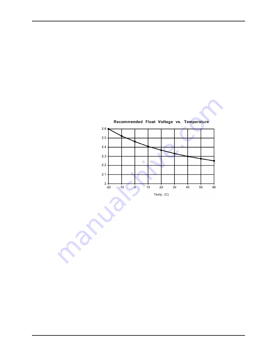
15.4.2 Float Voltage Regulation
When not in current limit, the controller regulates the VFBK pin to +2.5 volts
based on an internal reference. Resistors R25 and R28 attenuate the output
voltage to 2.5 volts DC. The thermistor R52 in series with R51 provides voltage
setpoint modulation based on the thermistor resistance. The nominal regulated
voltage setpoint at 25
ø
C is 7.05 volts DC. With a 3-cell battery, the nominal
charged cell voltage is thus 2.35 volts at 25
ø
C. The temperature compensation
of the battery charger adjusts the output voltage to match (three times) the
recommended charged cell voltage as shown in Figure 15-6.
Figure 15-6: Float Voltage vs. Temperature
Capacitor C42, resistor R27, and capacitor C24 provide frequency compensation
for the voltage error amplifier.
15.4.3 Drive Translator
The switch control output of the controller does not drive the buck switch
directly, but through the inverting driver U3. The series buck switch is
P-channel FET Q2. The switch is on when the gate is pulled down toward
ground from the DC input rail. Because the gate voltage rating is limited to
15 volts, and the charger input voltage (DCSRC) may exceed 18 volts, we have
added a driver voltage regulator consisting of emitter follower Q5 with Zener
D9, which keeps the voltage from driver U3 limited to 12 volts under all input
voltage conditions. Diode D7 couples the switch control signal from the
controller to the driver.
15.5 POWER DEVICES
The switch connects the input source to inductor L3 through current transformer
T2 and a section of diode D10. A second section of D10 acts as the "catch"
diode in the buck converter. The output voltage is built up across C20 and
applied directly to the battery. The series section of diode D10 has been added
Summary of Contents for NELLCOR NPB-4000
Page 66: ... THIS PAGE INTENTIONALLY LEFT BLANK ...
Page 68: ...Section 7 Spare Parts 7 2 Figure 7 1 NPB 4000 C Top Assembly Drawing ...
Page 70: ...Section 7 Spare Parts 7 4 Figure 7 2 NPB 4000 C Front Case Assembly Diagram Sheet 1 of 2 ...
Page 72: ...Section 7 Spare Parts 7 6 Figure 7 3 NPB 4000 C Front Case Assembly Diagram Sheet 2 of 2 ...
Page 74: ...Section 7 Spare Parts 7 8 Figure 7 4 NPB 4000 C Rear Case Assembly Diagram Sheet 1 of 2 ...
Page 76: ...Section 7 Spare Parts 7 10 Figure 7 5 NPB 4000 C Rear Case Assembly Diagram Sheet 2 of 2 ...
Page 78: ...Section 7 Spare Parts 7 12 Figure 7 6 NPB 4000 C Power Supply Heat Sink Assembly Diagram ...
Page 80: ... THIS PAGE INTENTIONALLY LEFT BLANK ...
Page 96: ... THIS PAGE INTENTIONALLY LEFT BLANK ...
Page 114: ... THIS PAGE INTENTIONALLY LEFT BLANK ...
Page 140: ... THIS PAGE INTENTIONALLY LEFT BLANK ...
Page 180: ... THIS PAGE INTENTIONALLY LEFT BLANK ...
Page 192: ... THIS PAGE INTENTIONALLY LEFT BLANK ...
Page 208: ... THIS PAGE INTENTIONALLY LEFT BLANK ...
Page 210: ... THIS PAGE INTENTIONALLY LEFT BLANK ...
Page 211: ...Section 17 Drawings 17 3 Figure 17 1 MP 205 PCB Schematic Sheet 1 of 2 ...
Page 212: ...Section 17 Drawings 17 5 Figure 17 2 MP 205 PCB Schematic Sheet 2 of 2 ...