


TR850 Service Manual
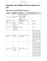
Analog&digit
al ACP
Observe ACP display value.
W:
<
-70dB
N:
<
-60dB
Spurious
emission
Observe spectrum analyzer display value.
<
1GHz:
<
-36dBm
>
1GHz:
<
-30dBm
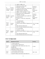
6.2.3. Rx Adjustment
Modulation
Subject
Modulation Procedure
Standard
Rx Sensitivity
1. Enter computer modulation mode.
2. Enter modulation mode ”Receiver BPF”, and click the six
frequencies one by one.
3. Make SINA
>
12dB.
4. Set the four Rx frequencies as -25.825MHz(*1
、
*2
、
*3
、
*4),
and signal strength as -40dBm; the SINA should be
<
7dB.
-
Narrow band
squelch level
9 on
1. Enter computer modulation mode
2. Set the channel to the current modulation frequency.
3. Enter modulation mode “SQL9 Open (N)”, and click “start”,
and change to the next frequency after the value is stable.
4. Modualte the frequency of narrow band and wide band in
turn.
-
Narrow band
squelch level
9 off
1. Enter computer modulation mode.
2. Set the channel to the current modulation mode.
3. Enter the modulation mode ”SQL9 Close(N)”, and click
“start”, and change to the next frequency after the value is
stable.
4. Modulate the frequency of narrow band and wide band in
turn.
-
47
Summary of Contents for TR850
Page 1: ......
Page 45: ...TR850 Service Manual 5 4 Connection 1 2 3 4 6 8 7 5 9 10 13 14 15 16 18 17 11 12 41 ...
Page 90: ...TR850 Service Manual Figure 1 Rx Module Top Board PCB View 86 ...
Page 91: ...TR850 Service Manual Figure 2 Rx Module Bottom Board PCB View 87 ...
Page 93: ...TR850 Service Manual Figure 5 Power Amplifier Module Bottom Board PCB View 89 ...
Page 94: ...TR850 Service Manual Figure 6 Baseband Mainboard Top Board PCB View 90 ...
Page 95: ...TR850 Service Manual Figure 7 Baseband Mainboard Bottom Board PCB View 91 ...
Page 97: ...TR850 Service Manual Figure 10 Power Board Top Board PCB View 93 ...
Page 114: ...TR850 Service Manual Figure 16 Baseband Mainbaord Schematic Diagram 110 ...
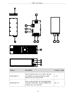
Page 169: ...TR850 Service Manual Figure 1 Rx module Top Board Position Mark Diagram 165 ...
Page 170: ...TR850 Service Manual Figure 2 Rx Module Buttom Board Position Mark Diagram 166 ...
Page 172: ...TR850 Service Manual Figure 5 Power Amplifier Module Buttom Position Mark Diagram 168 ...
Page 173: ...TR850 Service Manual Figure 6 Baseband Mainboard Top Board Position Mark Diagram 169 ...
Page 174: ...TR850 Service Manual Figure 7 Baseband Mainboard Buttom Board Position Mark Diagram 170 ...
Page 176: ...TR850 Service Manual Figure 10 Power Board Top Board Position Mark Diagram 172 ...
Page 193: ...TR850 Service Manual Figure 16 Baseband Mainboard Schematic Diagram 189 ...