


TR850 Service Manual
and either one of them can be selected.
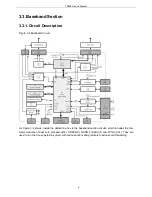
J8 is the interface and SMA of GPS interface, and it supports active antenna with 3.3V feed output.
J9 is the ACCY external interface provided by baseband, and it is used for function expansion or test.
It includes the input and output of local speech, external PTT, and programmable expansion IO. It provides
12V/1A DC output.
J15 is the interface of Rx board, including digital IF, SPI interface signal, 12C interface signal for storing
data of test and adjustment, etc.
J17 is the interface of Tx board, including two point modulation signal, SPI interface of Tx circuit PLL, Tx
control signal, etc.
J18 is the control interface of RF power amplifier, including SWR , TEMP_DET, POWER_CONTROL,
TX_ENABLE, etc.
J19 is the interface of LED status display board.
J20 is the 12VDC fan interface.The fan will be switched on when the radio transmits or the temperature
goes beyond the set range.
J23 is the serial port UART2.
LED2
、
LED3
、
LED4
、
LED5 indicates program operation status.
LED6 indicates CPU power.
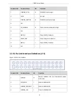
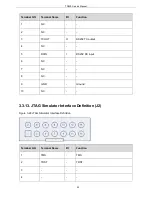
3.3.8. Tx Unit Interface Definition (J17)
Figure 3-17 Tx Unit Interface Definition
Terminal NO.
Terminal Name
I/O
Function
1
GND
-
Ground
2
MOD1
O
TX Modulate signal output1
3
GND
-
Ground
4
MOD2
O
TX Modulate signal output2
5
GND
-
Ground
18
Summary of Contents for TR850
Page 1: ......
Page 45: ...TR850 Service Manual 5 4 Connection 1 2 3 4 6 8 7 5 9 10 13 14 15 16 18 17 11 12 41 ...
Page 90: ...TR850 Service Manual Figure 1 Rx Module Top Board PCB View 86 ...
Page 91: ...TR850 Service Manual Figure 2 Rx Module Bottom Board PCB View 87 ...
Page 93: ...TR850 Service Manual Figure 5 Power Amplifier Module Bottom Board PCB View 89 ...
Page 94: ...TR850 Service Manual Figure 6 Baseband Mainboard Top Board PCB View 90 ...
Page 95: ...TR850 Service Manual Figure 7 Baseband Mainboard Bottom Board PCB View 91 ...
Page 97: ...TR850 Service Manual Figure 10 Power Board Top Board PCB View 93 ...
Page 114: ...TR850 Service Manual Figure 16 Baseband Mainbaord Schematic Diagram 110 ...
Page 169: ...TR850 Service Manual Figure 1 Rx module Top Board Position Mark Diagram 165 ...
Page 170: ...TR850 Service Manual Figure 2 Rx Module Buttom Board Position Mark Diagram 166 ...
Page 172: ...TR850 Service Manual Figure 5 Power Amplifier Module Buttom Position Mark Diagram 168 ...
Page 173: ...TR850 Service Manual Figure 6 Baseband Mainboard Top Board Position Mark Diagram 169 ...
Page 174: ...TR850 Service Manual Figure 7 Baseband Mainboard Buttom Board Position Mark Diagram 170 ...
Page 176: ...TR850 Service Manual Figure 10 Power Board Top Board Position Mark Diagram 172 ...
Page 193: ...TR850 Service Manual Figure 16 Baseband Mainboard Schematic Diagram 189 ...


