Platform Power Delivery Guidelines
164
Design Guide
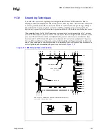
For an 8-layer board, refer to
in which the ground planes are used as signal reference
planes. If cost is the main consideration, you may opt to design a platform using fewer layers. In
that situation, a thorough analysis is recommended.
Power must be distributed as a plane. This plane can be constructed as an island on a layer used for
other signals, on a supply plane with other power islands, or as a dedicated layer of the PCB.
Processor power should never be distributed by traces alone.
Because processor voltage is unique to most system designs, a voltage island is probably be the
most cost-effective means of distributing power to the processors. This island should not have any
breaks from the source of power to the load to minimize inductance in the plane. It should
completely surround all of the pins of the source and all of the pins of the load.
Intel recommends a 2 oz. copper power plane for VCC_CPU, and a 2 oz. copper power plane for
VSS. This can be implemented on two 1 oz. copper layers or four 1/2 oz. copper layers. The bulk
capacitors can be placed close to the processors, and the high-frequency capacitors should be
placed next to the processors. Distribute the bulk and high-frequency capacitors equally on both
sides of the socket where the power/ground pins are located (the east and west side).
The Intel Xeon processor socket has 603 pins with 50 mil pitch. The routing of the signals, power,
and ground pins require creation of lots of vias. These vias cause a “Swiss cheese” effect in the
power and ground planes beneath the processor, resulting in increased inductance of these planes.
It is recommended that you place as many high-frequency capacitors as possible inside the cutout
of the processor socket. The remaining high-frequency capacitors should be placed next to the
processor, specifically near the power/ground pins.
The data bus must route over a uniform power plane because of signal quality constraints.
Consequently, in a multiprocessor system design, a single power plane should be used for power
delivery to all processors. Multiple processors operating at different voltages are not supported, and
will not be validated by Intel.
System boards can include a SENSE input for each Voltage Regulator. The trace resistance should
not be greater than 1.0
Ω
. The sense pins do not draw current, therefore no voltage drop exists.
Route the SENSE trace as follows:
•
In a DP system, the SENSE lines from the VR should be routed to a point between and
equidistant from all processors. At this point, tie all SENSE lines together and connect to
VCC_CPU. This will allow for proper current sharing between the VRs.
•
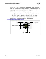
The processor VCCSENSE and VSSSENSE pins must be routed to vias. The vias should be as
close to the socket pins as possible, and should be connected with low impedance traces.
Because these signals provide measurement points to verify adherence to the processor's
VCC_CPU specifications, the vias need to be accessible to measurement equipment. These
pins must not be used as SENSE lines to the VRs.
12.2.4
Voltage Regulator Requirements
Intel requires a local VRM 9.1-compliant Voltage Regulator for VCC_CPU. As shown in
, it can be either one Voltage Regulator Module (VRM 9.1) DC-to-DC converter for
each processor, or one Voltage Regulator-Down (VRD) solution for both processors in a DP
system. Refer to either
VRM 9.1 DC-DC Converter Design Guidelines
or
Dual Intel
®
Xeon™
Processor Voltage Regulator Down (VRD) Design Guidelines
for Voltage Regulator tolerance
specifications (regulation requirements at the voltage regulator remote sense point located at the
geometric center of the processors). These two documents are referred to as the voltage regulator
guidelines.
Summary of Contents for Xeon
Page 24: ...Introduction 24 Design Guide This page is intentionally left blank ...
Page 30: ...Component Quadrant Layout 30 Design Guide This page is intentionally left blank ...
Page 52: ...Platform Clock Routing Guidelines 52 Design Guide This page is intentionally left blank ...
Page 66: ...System Bus Routing Guidelines 66 Design Guide This page is intentionally left blank ...
Page 118: ...Intel 82870P2 P64H2 118 Design Guide This page is intentionally left blank ...
Page 146: ...I O Controller Hub 146 Design Guide This page is intentionally left blank ...
Page 148: ...Debug Port 148 Design Guide This page is intentionally left blank ...
Page 210: ...Schematic Checklist 210 Design Guide This page is intentionally left blank ...
Page 220: ...Layout Checklist 220 Design Guide This page is intentionally left blank ...
Page 222: ...Schematics 222 Design Guide This page is intentionally left blank ...


