VT Camera Link series
Page 25 of 88
VW40-161-001
7.5
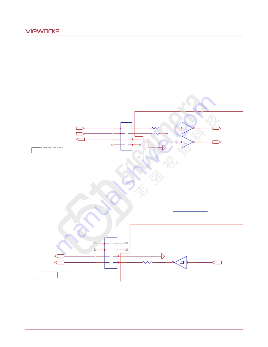
Trigger / Direction Input Circuit
The following figure shows trigger signal input and TDI direction input circuit of the 4 pin connector. Transmitted
trigger signal and TDI direction signal is applied to the internal circuit through a CMOS buffer with a good noise
margin. The minimum trigger width that can be recognized by the camera is 1
㎲
. If transmitted trigger signal is
less than 1
㎲
, the camera will ignore the trigger signal. An external trigger and TDI direction circuit example is
shown below.
Figure 7.5 Trigger / Direction Input Schematic
7.6
Strobe Output Circuit
The strobe output signal comes out through a 3.3 V output level of Line Driver IC. A pulse width of the signal is
synchronized with a Line Start trigger (shutter) signal of the camera (refer to
).
Figure 7.6 Strobe Output Schematic
②
③
④
①
HR 10A-7R-4SB
Camera
USER
47 Ω
47 Ω
Trigger Input
Direction Input
Ground Signal
Trigger Input(LineIn0)
Direction Input (LineIn1)
Input High Level( 2 ~ 5V)
input Low Level ( 0 ~ 0.8 V)
②
③
④
①
HR 10A-7R-4SB
47 Ω
Strobe Out
Strobe Out
Ground Signal
Camera
USER
3.3V
0V
Summary of Contents for VT Series
Page 1: ......


