


2-31
Confidential
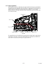
(3) Development
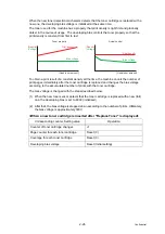
Toner is attracted to a printed-image area on the exposure drum where surface potential is
lowered due to exposure.
By controlling developing bias voltage supplied to the develop roller, the amount of toner
taken to the drum is adjusted to keep printing density constant.
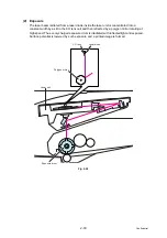
Fig. Ref. 2-31
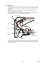
<Flow up of toner to the development process>
Toner adheres to the charged develop roller. Such adhered toner is adjusted to an even
thickness, and is attracted to an exposed area on the exposure drum.
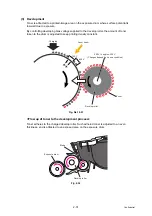
Fig. 2-32
Charging
400 V to approx. 300 V
(Changes depending on use condition)
Toner
Develop roller
Laser beam
150 V
850 V
Blade
Exposure drum
Develop roller
Summary of Contents for DCP 8085DN
Page 13: ...CHAPTER 1 SPECIFICATIONS ...
Page 52: ...Confidential CHAPTER 2 THEORY OF OPERATION ...
Page 69: ...2 16 Confidential 3 3 Paper Feeding Fig 2 18 LT path DX path MP path Paper tray path ...
Page 89: ...CHAPTER 3 ERROR INDICATION AND TROUBLESHOOTING ...
Page 178: ...Confidential CHAPTER 4 PERIODICAL MAINTENANCE ...
Page 248: ...CHAPTER 5 DISASSEMBLY REASSEMBLY ...
Page 265: ...5 12 Confidential Fig 5 7 EM2 4 places Separation pad ASSY ...
Page 501: ...Confidential CHAPTER 6 ADJUSTMENTS AND UPDATING OF SETTINGS REQUIRED AFTER PARTS REPLACEMENT ...
Page 507: ...6 5 Confidential 8 Alert warning message of WHQL appears Click Continue Anyway to proceed ...
Page 516: ...CHAPTER 7 SERVICE MODE ...
Page 525: ...7 7 Confidential For color scanning Fig 7 2 ...
Page 527: ...7 9 Confidential For white and black scanning Fig 7 3 ...
Page 528: ...7 10 Confidential For color scanning Fig 7 4 ...
Page 567: ...Confidential CHAPTER 8 CIRCUIT DIAGRAMS WIRING DIAGRAM ...
Page 569: ...8 1 Confidential 1 CIRCUIT DIAGRAMS High voltage Power Supply PCB Circuit Diagram Fig 8 1 ...
Page 570: ...8 2 Confidential LVPS PCB Circuit Diagram 230V Fig 8 2 ...
Page 571: ...8 3 Confidential LVPS PCB Circuit Diagram 115V Fig 8 3 ...


