375
2467S–AVR–07/09
ATmega128
3.
Updated
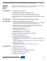
“External Memory Interface” on page 26
4.
Updated
“Device Identification Register” on page 253
.
5.
Updated
“Electrical Characteristics” on page 318
6.
Updated
“ADC Characteristics” on page 325
.
7.
Updated
“Typical Characteristics” on page 333
8.
Updated
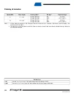
“Ordering Information” on page 368
.
Rev. 2467K-03/04
1.
Updated
Rev. 2467J-12/03
1.
Updated
“Calibrated Internal RC Oscillator” on page 42
Rev. 2467I-09/03
1.
“XTAL Divide Control Register – XDIV” on page 37
2.
Updated
“JTAG Interface and On-chip Debug System” on page 49
3.
Updated values for V
BOT
4.
Updated
“Test Access Port – TAP” on page 246
regarding JTAGEN.
5.
Updated description for the JTD bit on
.
6.
Added a note regarding JTAGEN fuse to
.
7.
Updated R
PU
values in
“DC Characteristics” on page 318
.
8.
Added a proposal for solving problems regarding the JTAG instruction IDCODE in
Rev. 2467H-02/03
1.
Corrected the names of the two Prescaler bits in the SFIOR Register.
2.
Added Chip Erase as a first step under
“Programming the Flash” on page 315
and
“Programming the EEPROM” on page 316
3.
Removed reference to the “Multipurpose Oscillator” application note and the “32 kHz
Crystal Oscillator” application note, which do not exist.
4.
5.
Various minor Timer1 corrections.
6.
Added information about PWM symmetry for Timer0 and Timer2.
7.
Various minor TWI corrections.
8.
Added reference to
from both SPI Serial Programming and Self
Programming to inform about the Flash Page size.

