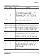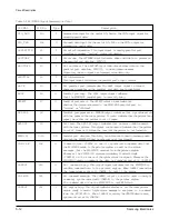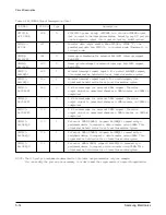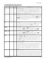
Table 1-1 KS32C6100 Signal Descriptions (Cont.)
S I G N A L
PIN No.
Type
Description
nWE[3:0]/
33~36
O
Not data write enable for SRAM/External IO. Whenever a memory
ExtMnDB[3:0]
access for SRAM/External IO occurs, the four nWE outputs indicate
the byte selections and control the write enable port of the specific
devices.
In external bus master mode, it acts as ExtMnDB[3:0] to indicate the
byte latch for external master accessing memory.
DA[12:0]
128~133
I/O
DA[12:0] acts as an output for the 13-bit DRAM address bus. In
/
135~141
external master mode, it acts as an input, in which ExtMA[27:24]
corresponds to the higher 4 bits out of 28-bit external master address
ExtMA[27:24]
128~131
bus ExtMA[27:0]; ExtMBST is burst mode selection signal; ExtMRnW
ExtMBST
138
is R/W control signal; and ExtMAS[1:0] is memory access size control
ExtMAS[1:0]
139~140
signal which is used to inform KS32C6100’s memory controller
ExtMRnW
141
that the external master will access memory in byte (00), halfword (10).
Note the state (11) for ExtMAS [1:0] is not used.
nRAS[5:0]
122~127
O
Not row address strobes for DRAM banks. The KS32C6100 supports
up to six DRAM banks. One nRAS output is provided for each bank.
nCAS[3:0]
116~118
O
Not column address strobes for DRAM. The four nCAS outputs
121
indicate the byte selections whenever a DRAM bank is accessed.
n D O E
115
O
Not output enable for DRAM. Whenever a DRAM access occurs,
the nOE output controls the output enable port of the specific DRAM.
n D W E
114
O
Not write enable for DRAM. Whenever a DRAM access occurs, the
nWE output controls the write enable port of the specific DRAM.
nSRD[1:0]
144, 146
O
Not special I/O read strobe with address latch.
nSWR[1:0]
145, 147
O
Not special I/O write strobe with address latch.
ExtMREQ
23
I
External master request. The ExtMREQ input signal indicates that
the external master requests to hold KS32C6100 system bus.
ExtMACK
24
O
Acknowledge for external master holding request. This output signal
indicates that the external master holding request has been accepted.
ExtMnDL
25
I/O
External master data latch signal.
U C L K
156
I
The external UART clock source input. Usually, MCLK is used as the
U A RT clock source.
R X D
151
I
Receive data input for the UART. RXD is the UART’s input signal for
receiving serial data.
D T R
149
I
Data terminal ready. DTR input signals the KS32C6100 that the
peripheral (or host) is ready to transmit or receive serial data.
T X D
150
O
Transmit data output for the UART. TXD is the UART’s output for
transmitting serial data.
D S R
148
O
Data set ready. DSR output signals the host (peripheral) that the
KS32C6100 UART is ready to transmit or receive serial data.
Samsung Electronics
5-11
Circuit Description
Содержание MSYS 5150
Страница 9: ...2 6 Samsung Electronics Specification Memo ...
Страница 16: ...3 26 Samsung Electronics Setup and Installing Memo ...
Страница 37: ...4 2 Samsung Electronics Theory of Operation ...
Страница 41: ...4 6 Samsung Electronics Memo Theory of Operation ...
Страница 116: ...Samsung Electronics 7 9 Maintenance Troubleshooting No Image ...
Страница 117: ...Samsung Electronics Maintenance Troubleshooting 7 10 ...
Страница 118: ...Samsung Electronics 7 11 Maintenance Troubleshooting All Black ...
Страница 119: ...7 12 Samsung Electronics Maintenance Troubleshooting Vertical White Line Band ...
Страница 120: ...Samsung Electronics 7 13 Maintenance Troubleshooting Dark Image ...
Страница 121: ...7 14 Samsung Electronics Maintenance Troubleshooting Background ...
Страница 122: ...Samsung Electronics 7 15 Maintenance Troubleshooting Ghost ...
Страница 123: ...7 16 Samsung Electronics Maintenance Troubleshooting Black Dot ...
Страница 124: ...Samsung Electronics 7 17 Maintenance Troubleshooting Horizontal Band ...
Страница 125: ...7 18 Samsung Electronics Maintenance Troubleshooting Irregular Density ...
Страница 126: ...Samsung Electronics 7 19 Maintenance Troubleshooting White Spot ...
Страница 127: ...7 20 Samsung Electronics Maintenance Troubleshooting Trembling at the End When OHP Printing ...
Страница 128: ...Samsung Electronics 7 21 Maintenance Troubleshooting Poor Fusing Grade ...
Страница 132: ...Samsung Electronics 7 25 Maintenance Troubleshooting No Power LCD NO display LED Off ...
Страница 133: ...Fuser Error 7 26 Samsung Electronics Maintenance Troubleshooting ...
Страница 134: ...Samsung Electronics 7 27 Maintenance Troubleshooting Paper Jam Mis feeding ...
Страница 135: ...7 28 Samsung Electronics Maintenance Troubleshooting Paper Jam Jam1 ...
Страница 136: ...Samsung Electronics Maintenance Troubleshooting 7 29 Engine Error ...
Страница 137: ...7 30 Samsung Electronics Maintenance Troubleshooting Memo ...
Страница 187: ...9 28 Samsung Electronics Electrical Parts List ...
Страница 189: ...11 Connection Diagram Samsung Electronics 11 1 ...
Страница 190: ...12 1 Main Circuit Diagram Samsung Electronics 12 1 12 Schematic Diagrams ...
Страница 191: ...Schematic Diagrams 12 2 Samsung Electronics Main Circuit Diagram ...
Страница 192: ...Main Circuit Diagram Samsung Electronics 12 3 Schematic Diagrams ...
Страница 193: ...Schematic Diagrams 12 4 Samsung Electronics Main Circuit Diagram ...
Страница 194: ...Main Circuit Diagram Samsung Electronics 12 5 Schematic Diagrams ...
Страница 195: ...Schematic Diagrams 12 6 Samsung Electronics Main Circuit Diagram ...
Страница 196: ...Main Circuit Diagram Samsung Electronics 12 7 Schematic Diagrams ...
Страница 200: ...12 3 Sensors Circuit Diagram Samsung Electronics 12 11 Schematic Diagrams ...
Страница 201: ...Schematic Diagrams 12 12 Samsung Electronics 12 4 Switch Circuit Diagram ...
Страница 202: ...Samsung Electronics 12 13 Schematic Diagrams 12 5 Joint Circuit Diagram ...
Страница 203: ...Schematic Diagrams 12 14 Samsung Electronics 12 6 OPE Circuit Diagram IF Active HIGH Logic IF Active LOW Logic ...
Страница 204: ...Samsung Electronics 12 15 Schematic Diagrams 12 7 PTL Circuit Diagram ...
Страница 205: ...Schematic Diagrams 12 16 Samsung Electronics 12 8 SCAN Circuit Diagram ...
Страница 206: ...Samsung Electronics 12 17 Schematic Diagrams 12 9 Engin Circuit Diagram ...
Страница 207: ...Schematic Diagrams 12 18 Samsung Electronics Engin Circuit Diagram ...
Страница 208: ...Samsung Electronics 12 19 Schematic Diagrams 12 10 LIU Circuit Diagram ...
Страница 210: ... Samsung Electronics Co Ltd Mar 1999 Printed in Korea P N JC68 00097A Rev 1 00 ELECTRONICS ...


