


Section 24 Flash Memory
Rev. 1.00 Apr. 28, 2008 Page 801 of 994
REJ09B0452-0100
24.10 Switching between User MAT and User Boot MAT
It is possible to switch between the user MAT and user boot MAT. However, the following
procedure is required because both of these MATs are allocated to address 0.
(Switching to the user boot MAT disables programming and erasing. Programming of the user
boot MAT should take place in boot mode or programmer mode.)
1. MAT switching by FMATS should always be executed from the on-chip RAM.
2. To ensure that switching has finished and access is made to the newly switched MAT, execute
four NOP instructions in the same on-chip RAM immediately after writing to FMATS (this
prevents access to the flash memory during MAT switching).
3. If an interrupt has occurred during switching, there is no guarantee of which memory MAT is
being accessed.
Always mask the maskable interrupts before switching between MATs. In addition, configure
the system so that NMI interrupts do not occur during MAT switching.
4. After the MATs have been switched, take care because the interrupt vector table will also have
been switched.
5. Memory sizes of the user MAT and user boot MAT are different. Do not access a user boot
MAT in a space of 8 kbytes or more. If access goes beyond the 8-kbyte space, the values read
are undefined.
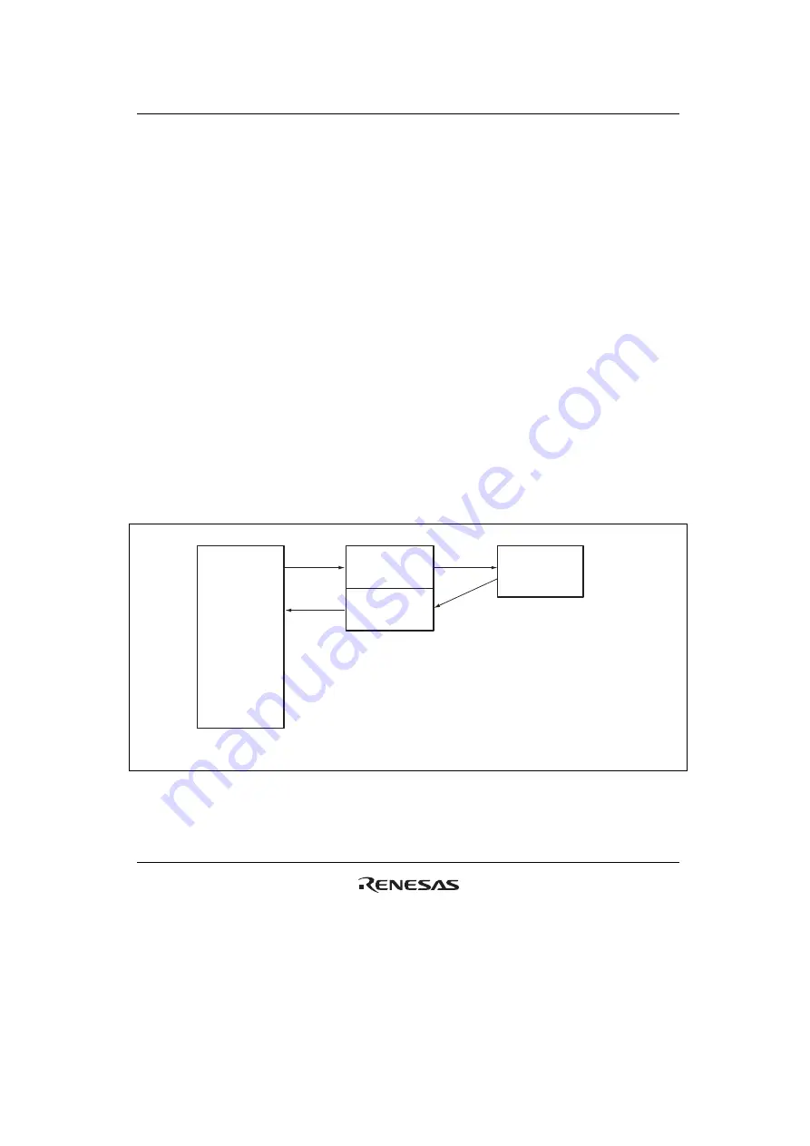
<User MAT>
<On-chip RAM>
<User boot MAT>
Procedure for
switching to
user boot MAT
Procedure for
switching to
user MAT
Procedure for switching to user boot MAT:
Procedure for switching to user MAT:
1. Disable interrupts (mask).
2. Write H'AA to FMATS.
3. Execute four NOP instructions before accessing the user boot MAT.
1. Disable interrupts (mask).
2. Write a value other than H'AA to FMATS.
3. Execute four NOP instructions before accessing the user MAT.
Figure 24.17 Switching between User MAT and User Boot MAT
Содержание H8S/2100 Series
Страница 2: ...Rev 1 00 Apr 28 2008 Page ii of xxvi...
Страница 54: ...Section 1 Overview Rev 1 00 Apr 28 2008 Page 28 of 994 REJ09B0452 0100...
Страница 92: ...Section 2 CPU Rev 1 00 Apr 28 2008 Page 66 of 994 REJ09B0452 0100...
Страница 158: ...Section 5 Interrupt Controller Rev 1 00 Apr 28 2008 Page 132 of 994 REJ09B0452 0100...
Страница 244: ...Section 8 8 Bit PWM Timer PWMU Rev 1 00 Apr 28 2008 Page 218 of 994 REJ09B0452 0100...
Страница 330: ...Section 10 16 Bit Timer Pulse Unit TPU Rev 1 00 Apr 28 2008 Page 304 of 994 REJ09B0452 0100...
Страница 354: ...Section 11 16 Bit Cycle Measurement Timer TCM Rev 1 00 Apr 28 2008 Page 328 of 994 REJ09B0452 0100...
Страница 380: ...Section 12 16 Bit Duty Period Measurement Timer TDP Rev 1 00 Apr 28 2008 Page 354 of 994 REJ09B0452 0100...
Страница 416: ...Section 13 8 Bit Timer TMR Rev 1 00 Apr 28 2008 Page 390 of 994 REJ09B0452 0100...
Страница 494: ...Section 15 Serial Communication Interface SCI Rev 1 00 Apr 28 2008 Page 468 of 994 REJ09B0452 0100...
Страница 612: ...Section 18 I 2 C Bus Interface IIC Rev 1 00 Apr 28 2008 Page 586 of 994 REJ09B0452 0100...
Страница 706: ...Section 20 LPC Interface LPC Rev 1 00 Apr 28 2008 Page 680 of 994 REJ09B0452 0100...
Страница 752: ...Section 21 FSI Interface Rev 1 00 Apr 28 2008 Page 726 of 994 REJ09B0452 0100...
Страница 774: ...Section 23 RAM Rev 1 00 Apr 28 2008 Page 748 of 994 REJ09B0452 0100...
Страница 1008: ...Section 28 Electrical Characteristics Rev 1 00 Apr 28 2008 Page 982 of 994 REJ09B0452 0100...
Страница 1020: ...Rev 1 00 Apr 28 2008 Page 994 of 994 REJ09B0452 0100...
Страница 1023: ......
Страница 1024: ...H8S 2117R Group Hardware Manual...


