


Chapter 16
BLE click board
This chapter introduces the features of the BLE P click board and how to use it on NXP's LS1028A reference design board (RDB)
16.1 Introduction
BLE P click carries the nRF8001 IC that allows you to add Bluetooth 4.0 to your device. The click communicates with the target
board MCU through mikroBUS
™
SPI (CS, SCK, MISO, MOSI), RDY and ACT lines, and runs on 3.3 V power supply.
BLE P click features a PCB trace antenna, designed for the 2400 MHz to 2483.5 MHz frequency band. The maximum device
range is up to 40 meters in open space.
16.2 Features
Following are the features provided by BLE P clickboard:
• nRF8001 Bluetooth low energy RF transceiver
— 16 MHz crystal oscillator
— Ultra-low peak current consumption <14 mA
— Low current for connection-oriented profiles, typically 2 μA
• PCB trace antenna (2400-2483.5 MHz, up to 40 meters)
• BLE Android app
• Interface: SPI (CS, SCK, MISO, MOSI), RDY and ACT lines
• 3.3 V power supply
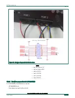
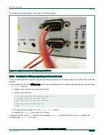
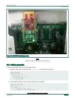
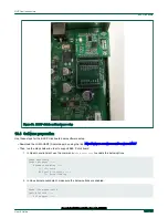
16.3 Hardware preparation
Use the following hardware items for the BLE P click board demo setup:
1. LS1028ARDB
2. BLE P Click board
3. Android phone (option)
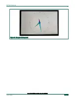
The figure below depicts the hardware setup required for the demo:
NXP Semiconductors
Open Industrial User Guide, Rev. 1.8, 05/2020
User's Guide
185 / 199