


Index
©
National Instruments Corporation
I-3
L
LED
Access LED, 3-4
Active LED, 3-4
LED
M
maximum signal rating (caution), 3-6
N
National Instruments
calibration certificate, B-2
customer education, B-1
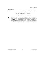
Declaration of Conformity, B-1
professional services, B-1
system integration services, B-1
technical support, B-1
worldwide offices, B-2
NI PXI-6653
configuration, 2-2
connectors, 3-5
functional overview, 3-6
installation
parts locator diagram, 3-3
signal descriptions (table), 3-6
O
OCXO
clock generation, 3-8
OCXO clock
signal description (table), 3-6
using the PXI_CLK10 PLL, 3-18
overview, 3-8
specifications, A-5
online technical support, B-1
oven-controlled crystal oscillator.
OCXO
P
PFI
PFI <0..5> connector
description, 3-5
location (diagram), 3-3
signal description (table), 3-7
PFI <0..5> signals
asynchronous routing, 3-16
front panel PFIs as inputs, 3-12
front panel triggers as outputs, 3-12
specifications, A-3
using front panel PFIs as inputs, 3-12
using front panel PFIs as outputs, 3-12
See
PLL
phone technical support, B-2
physical specifications, A-5
PLL
Active LED, 3-5
routing from the CLKIN connector, 3-5
using the PXI_CLK10 PLL, 3-18
power requirement specifications, A-6
professional services, B-1
programmable function interface.
PFI
programming examples, B-1
PXI backplane clock, 3-8
PXI star trigger bus.
See
PXI_STAR<0..12>
PXI star triggers
front panel triggers as outputs, 3-12
See
PXI_TRIG<0..7>
PXI_CLK10
Active LED, 3-5
clock generation, 3-8
DDS phase-lock, 3-7
front panel triggers as outputs, 3-12
routing to the CLKOUT connector, 3-5
using front panel PFIs as outputs, 3-13


