


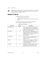


Chapter 3
Hardware Overview
©
National Instruments Corporation
3-7
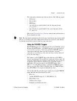
The remainder of this chapter describes how these signals are used,
acquired, and generated by the NI 6653 hardware, and explains how you
can route the signals between various locations to synchronize multiple
measurement devices and PXI chassis.
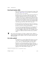
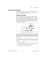
Clock Generation
The NI 6653 can generate two types of clock signals. The first clock is
generated using the onboard DDS chip, and the second is generated with a
precise 10 MHz oscillator. The following sections describe the two types
of clock generation and explain the considerations for choosing either type.
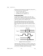
DDS Clock
Out
This is the output of the NI 6653 DDS. The DDS
frequency can be programmed with fine
granularity from 1 Hz to 80 MHz. The DDS chip
automatically phase-locks to PXI_CLK10.
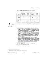
PXI_STAR<0..12>
In/Out
The PXI star trigger bus connects Slot 2 to
Slot<3..15> in a star configuration. The electrical
paths of each star line are closely matched to
minimize intermodule skew. An NI 6653 in
Slot 2 can route signals to Slots 3–15 using the
star trigger bus.
PFI <0..5>
In/Out
The Programmable Function Interface pins on
the NI 6653 route timing and triggering signals
between multiple PXI chassis. A wide variety of
input and output signals can be routed to or from
the PFI lines.
PXI_TRIG<0..7>
In/Out
The PXI trigger bus consists of eight digital lines
shared among all slots in the PXI chassis. The
NI 6653 can route a wide variety of signals to
and from these lines.
Note:
PXI_TRIG<0..5> are also known as RTSI
<0..5> in some hardware devices and APIs.
However, PXI_TRIG<6..7> are
not
identical to
RTSI<6..7>.
1
This feature is not supported in version 1.0 of the NI 6653 Driver Software.
Table 3-3.
Signal Descriptions (Continued)
Signal Name
Direction
Description


