


Chapter 3
Hardware Overview
©
National Instruments Corporation
3-17
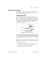
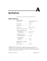
synchronization clock and distributes it to the modules in each chassis at
the same time. Synchronous routing can thus remove uncertainty about
when triggers are received. If the delays through the system are such that
an asynchronous trigger might arrive near the edge of the receiver clock, the
receiver might see the signal in the first clock cycle, or it might see it in the
second clock cycle. However, by synchronizing the signal, you can
eliminate the ambiguity, and the signal will always be seen in the second
clock cycle.
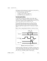
One useful feature of synchronous routing is that the signal can be
propagated on either the rising or falling edge of the synchronization clock.
In addition, the polarity of the destination signal can be inverted, which is
useful when handling active-low digital signals.
Possible sources for synchronous routing include the following sources:
•
Any front panel PFI pin
•
Any PXI star trigger line (PXI_STAR<0..12>)
•
Any PXI/RTSI trigger line (PXI_TRIG<0..7>)
•
Global software trigger
•
The synchronization clock itself
Note
The possible destinations for a synchronous route are identical to those for an
asynchronous route. The destinations include any front panel PFI pin, any PXI star trigger
line, or any PXI/RTSI trigger line.
The synchronization clock for a synchronous route can be any of the
following signals:
•
10 MHz PXI backplane clock signal
•
DDS clock on the NI 6653
•
Front panel
PFI 0
input
•
One of two “divided copies” of any of the above three signals. The
NI 6653 includes two clock-divider circuits that can divide the
synchronization clock signals by any power of 2 up to 512.
Refer to the Figures 3-3 and 3-4 for an illustration of how the NI 6653
performs synchronous routing operations.


