


Chapter 3
Hardware Overview
3-14
ni.com
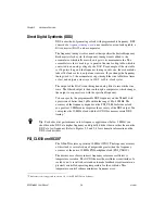
The backplane synchronization clock may be any of the following signals:
•
DDS clock
•
PXI_CLK10
•
PFI 0
Input
•
Any of the above signals divided by the first frequency divider
(2
n
, up to 512)
•
Any of the above signals divided by the second frequency divider
(2
m
, up to 512)
Refer to the
section for more information
about the synchronization clock.
Note
The backplane synchronization clock is the same for all routing operations in which
PXI/RTSI <0..5> is defined as the output, although the divide-down ratio for this clock
(full rate, first divider, second divider) may be chosen on a per route basis.
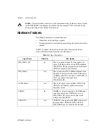
Using the PXI Star Triggers
There are up to 13 PXI star triggers per chassis. Each trigger line is a
dedicated connection between Slot 2 and one other slot. The
PXI Specification, Revision 2.0
, requires that the propagation delay along
each star trigger lines be matched to within 1 ns. A typical upper limit for
the skew in most PXI chassis is 500 ps. The low skew of the PXI star trigger
bus is useful for applications that require triggers to arrive at several
modules nearly simultaneously.
The star trigger lines are bidirectional, so signals can be sent to Slot 2 from
a module in another slot or from Slot 2 to the other module.
You can independently select the output signal source for each PXI star
trigger line from one of the following sources:
•
PFI <0..5>
•
PXI/RTSI triggers <0..7> (PXI_TRIG<0..7>)
•
Another PXI star trigger line (PXI_STAR <0..12>)
•
Global software trigger
•
Backplane synchronization clock
Refer to the
section for more information on
the backplane synchronization clock.


