


Chapter 3
Hardware Overview
©
National Instruments Corporation
3-9
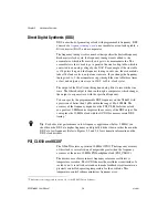
An NI 6653 module located in Slot 2 of a PXI chassis can replace the native
PXI 10 MHz backplane frequency reference clock (PXI_CLK10) with the
more stable and accurate output of the OCXO. All other PXI modules in the
chassis that reference the 10 MHz backplane clock benefit from this more
accurate frequency reference. Furthermore, the DDS chip on the NI 6653
references its output to the backplane clock and also takes advantage of the
superior OCXO accuracy. The OCXO does not automatically replace the
native 10 MHz clock; this feature must be explicitly enabled in software
1
.
The OCXO output can also be routed out to the
CLKOUT
connector
1
.
In addition to replacing the native backplane clock directly, the OCXO can
phase lock to an external frequency source. This operation is discussed in
detail in the
section.
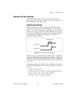
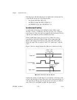
Routing Signals
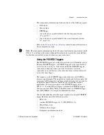
The NI 6653 has versatile trigger routing capabilities. It can route signals
to and from the front panel, the PXI star triggers, and the
PXI/RTSI triggers.
The NI 6653 also can route a 10 MHz clock from
CLKIN
to the PXI
10 MHz reference clock, or it can lock the OCXO to an external reference
clock and send that to the PXI 10 MHz reference clock. The NI 6653 can
route either the OCXO or the PXI 10 MHz reference clock to
CLKOUT
1
.
Figures 3-3 and 3-4 summarize the routing features of the NI 6653.
The remainder of this chapter details the capabilities and constraints of
the routing architecture.
1
This feature is not supported in version 1.0 of the NI 6653 Driver Software.


