


Chapter 3
Hardware Overview
3-6
ni.com
Caution
Connections that exceed any of the maximum ratings of input or output signals
on the NI PXI-6653 can damage the module and the computer. NI is
not
liable for any
damage resulting from such signal connections.
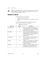
Hardware Features
The NI 6653 performs two broad functions:
•
Generating clock and trigger signals
•
Routing internally or externally generated signals from one location to
another
Table 3-3 outlines the function and direction of the signals that are
discussed in detail in the remainder of this chapter.
Table 3-3.
Signal Descriptions
Signal Name
Direction
Description
PXI_CLK10_IN
1
In
This is an internal signal that can replace the
native 10 MHz oscillator on the PXI backplane.
PXI_CLK10_IN may originate from the onboard
OCXO or from an external source.
PXI_CLK10
Out
This signal is the PXI 10 MHz backplane clock.
By default, this signal is the output of the native
10 MHz oscillator in the chassis. An NI 6653 in
Slot 2 can replace this signal with
PXI_CLK10_IN.
OCXO Clock
1
Out
This is the output of the 10 MHz OCXO. The
OCXO is an extremely stable and accurate
frequency source.
CLKIN
1
In
CLKIN is a signal connected to the SMB input
pin of the same name. CLKIN can serve as
PXI_CLK10_IN or be used as a phase lock
reference for the OCXO.
CLKOUT
1
Out
CLKOUT is the signal on the SMB output pin of
the same name. Either the OCXO clock or
PXI_CLK10 may be routed to this location.


