


©
National Instruments Corporation
I-1
Index
A
Access LED, 3-4
Active LED
color explanation (table), 3-5
overview, 3-4
asynchronous routing
overview, 3-15
sources and destinations, 3-16
timing diagram, 3-15
B
backplane synchronization clock
possible sources, 3-14
using the PXI/RTSI triggers, 3-13
block diagram
NI 6653 functional overview, 3-2
routing architecture, 3-10
signal selection circuitry, 3-10
C
cable configuration, 3-12
calibration certificate, B-2
changing the Active LED color (tip), 3-4
CLKIN connector
description, 3-5
location (diagram), 3-3
signal description (table), 3-6
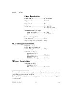
specifications, A-1
CLKOUT connector
description, 3-5
location (diagram), 3-3
signal description (table), 3-6
specifications, A-2
clock generation
DDS, 3-8
overview, 3-7
PXI_CLK10 and OCXO, 3-8
color
Access LED color explanation (table), 3-4
Active LED color explanation (table), 3-5
configuring the device
Access LED, 3-4
Active LED, 3-4
overview, 2-2
contacting National Instruments, B-2
conventions used in the manual,
customer
education, B-1
professional services, B-1
technical support, B-1
D
DDS
clock generation, 3-8
DDS clock
backplane synchronization clock, 3-14
front panel synchronization clock, 3-13
routing to the CLKOUT connector, 3-5
front panel triggers as outputs, 3-12
jitter performance (note), 3-8
signal description (table), 3-7
specifications, A-5
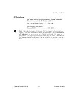
Declaration of Conformity, B-1
destinations
possible destinations (table), 3-11
diagnostic resources, B-1
direct digital synthesis.
See
DDS


