


©
National Instruments Corporation
A-1
A
Specifications
All specifications are typical at 25 °C unless otherwise noted.
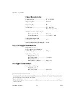
CLKIN Characteristics
CLKIN fundamental
frequency range
1
.................................... 1 MHz to 100 MHz, sine or
square wave
Input impedance ..................................... 50
Ω
±5%
Input coupling ........................................ AC
Voltage range ......................................... 400 mV
p-p
to 5 V
p-p
Absolute maximum input voltage
2
......... 6 V
p-p
, max
CLKIN to PXI_CLK10_IN delay
Uncompensated............................... 11 ns to 11.7 ns
PLL compensated ........................... ±1 ns, max
CLKIN frequency accuracy
For PLL and OCXO........................ ±1.5 ppm
Jitter added to CLKIN
Without PLL ................................... 15 ps
rms
With PLL ........................................ 2.5 ps
rms
Duty cycle distortion of CLKIN
without PLL ........................................... +1%
Duty cycle of PLL.................................. 45 to 55%
1
CLKIN fundamental frequency can be any multiple of 1 MHz within the range specified when the PLL is engaged and
PXI_CLK10 is locking to it. The frequency must be 10 MHz when replacing PXI_CLK10 without the PLL.
2
Stresses beyond those listed can cause permanent damage to the device. Exposure to absolute maximum rated conditions for
extended periods of time can affect device reliability. Functional operation of the device outside the conditions indicated in
the operational parts of the specification is not implied.


