


Appendix A
Specifications
©
National Instruments Corporation
A-3
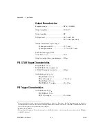
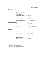
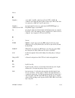
PFI<0..5>
Input Characteristics
Frequency range ..................................... DC to 100 MHz
Input impedance ..................................... 50
Ω
±5% or 1 k
Ω
±5%,
software-selectable
Input coupling ........................................ DC
Voltage level .......................................... 0 to 5 V
Absolute maximum input voltage
1
System powered off ........................ ±7 V, max
System powered on ......................... –7 to +5.5 V max
Input threshold
Voltage level ................................... 0.3 to 4.3 V, software-selectable
Voltage resolution........................... 20 mV (8 bits)
Error ................................................ ±40 mV
Hysteresis ............................................... 10 mV
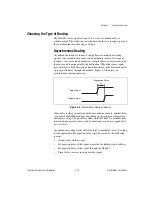
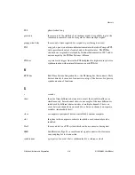
Asynchronous delay, t
pd
PFI <0..5> to
PXI_TRIG<0..7> output ................. 16 to 23 ns
PFI <0..5> to
PXI_STAR<0..12> output .............. 11 to 12.5 ns
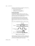
Synchronized trigger
input setup time, t
setup
2
........................... 8 ns
Synchronized trigger
input hold time, t
hold
2
.............................. 8 ns
1
Stresses beyond those listed can cause permanent damage to the device. Exposure to absolute maximum rated conditions for
extended periods of time can affect device reliability. Functional operation of the device outside the conditions indicated in
the operational parts of the specifications is not implied.
2
Relative to PXI_CLK10.


