


Chapter 3
Hardware Overview
3-18
ni.com
Generating a Single Pulse (Global SoftwareTrigger)
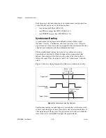
The global software trigger is a single pulse with programmable delay that
is fired on a software command. This signal is always routed synchronously
with a clock. Therefore, asynchronous routing is not supported when the
signal source is the global software trigger.
The software trigger can be delayed by up to 15 clock cycles on a per route
basis. This feature is useful if a single pulse must be sent to several
destinations with significantly different propagation delays. By delaying
the pulse on the routes with shorter paths, you can compensate for the
propagation delay. An example of such a situation would be when a trigger
pulse must arrive nearly simultaneously at the local backplane and the
backplane of another chassis separated by 50 meters of coaxial cable.
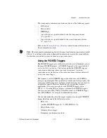
Using the PXI_CLK10 PLL
1
A module in Slot 2 of a PXI chassis can replace the PXI_CLK10 reference
clock. The NI 6653 offers three options for this replacement. This section
describes each of those options.
•
The first option is to directly replace PXI_CLK10 with the OCXO
output. This oscillator is a more stable and accurate reference than the
native backplane clock.
•
The second option is to route a 10 MHz clock directly from the front
panel to PXI_CLK10_IN, which is the pin on the backplane that will
replace PXI_CLK10. There is a delay through the module, as well as
a distribution delay on the backplane. These delays tend to be similar
for chassis of the same model, so routing the same clock to a pair of
chassis usually matches PXI_CLK10 to within a few nanoseconds.
•
The third option is to employ the NI 6653 PLL circuitry for the OCXO.
As in option 1, the output of the OCXO replaces the native 10 MHz
signal. However, this scheme also requires an input signal on
CLKIN
.
This signal must be a stable clock, and its frequency must be a multiple
of 1 MHz (5 MHz or 13 MHz, for example). The PLL feedback circuit
generates a voltage proportional to the phase difference between the
reference input on PXI_CLK10 and the output of the OCXO itself.
This PLL voltage output then tunes the output frequency of the OCXO.
As long as the incoming signal is a stable 1 MHz frequency multiple,
the PLL circuit quickly locks the OCXO to the reference, eliminating
all phase drift between the two signals.
1
The PXI_CLK10 PLL is not supported with version 1.0 of the NI 6653 Driver Software.


