


38
(9) Detune the signal generator above and below 21.4 Mc. to produce a maximum positive
and negative output. These voltages should be equal and have a magnitude of approximately
+/- 8 Volts, D.C. Minor adjustment of the primary of T-508 will cause the two peak voltages
to become exactly equal.
d. IF Amplifiers (CW Method).
(1) The characteristics of cascaded, critically coupled amplifier stages are such as to make
alignment difficult; however, the advantages of response stability, gain, and adjacent-channel
selectivity make this type of coupling most desirable. Alignment has been kept as simple as
possible by designing the three capacitively coupled double-tuned IF transformers,
comprising T-501, T-502, T-503, T-504, T-505 and T-506, to have almost identical
characteristics.
The primary and secondary Q's have been kept high, and therefore the mutual coupling is low
for the required bandwidth. These factors suggest a rather simple alignment procedure with a
minimum of equipment. The resonant frequency of the primary or the secondary in the
absence of the other (no couplings) is very nearly the proper tuning when the circuits are
coupled. If the primary circuit is detuned, the secondary adjusted for maximum output, and
the primary then returned to maximum, the overall response will be approximately correct.
This procedure is as follows:
(2) Remove the oscillator tube (V-204) to prevent mixing at the signal generator harmonic
frequencies.
(3) Set the receiver dial to approximately 60 Mc.
(4) Set the generator to 21.4 Mc. and connect to pin 1 of V-203.
(5) Connect a high-resistance DC voltmeter (VTVM) to the second limiter (V-504) grid
return.
(6) Set the generator output level to produce approximately 2 v on the VTVM.
(7) If the IF amplifier is known to be considerably out of adjustment, it will be necessary to
peak T-501, T-502, T-503, T-504, T-505 and T-506, to provide adequate gain.
(8) Detune the primary (T-505) counterclockwise against the stop.
Содержание G-187
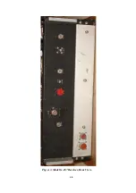
Страница 7: ...7 Figure 1 1 Model G 187 Special Purpose Receiver Front View...
Страница 9: ...9 Table 1 2 Semiconductor and Tube Complement...
Страница 10: ...10 Table 1 2 Semiconductor and Tube Complement continued...
Страница 14: ...14 Fig 2 1 Block Diagram Model G 187 Receiver...
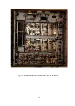
Страница 44: ...44 Fig 4 1 Model G 187 Receiver Top View Cover Removed...
Страница 45: ...45 Fig 4 2 Model G 187 Receiver Bottom View Covers Removed...
Страница 46: ...46 Fig 4 3 Model G 187 Receiver Rear View...
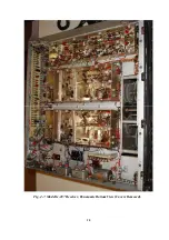
Страница 47: ...47 Fig 4 4 Model G 187 Receiver Panoramic Top View Cover Removed...
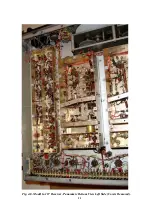
Страница 48: ...48 Fig 4 5 Model G 187 Receiver Panoramic Top View Left Side Cover Removed...
Страница 49: ...49 Fig 4 6 Model G 187 Receiver Panoramic Top View Right Side Cover Removed...
Страница 50: ...50 Fig 4 7 Model G 187 Receiver Panoramic Bottom View Covers Removed...
Страница 51: ...51 Fig 4 8 Model G 187 Receiver Panoramic Bottom View Left Side Covers Removed...
Страница 52: ...52 Fig 4 9 Model G 187 Receiver Panoramic Bottom View Right Side Covers Removed...
Страница 53: ...53 Table 4 2 Model G 187 Receiver Component Boards Lists...
Страница 54: ...54 Fig 4 10 Model G 187 Receiver Large Component Board...
Страница 56: ...56 Fig 4 14 Model G 187 Receiver Master Slave RF Tuners Top View...
Страница 57: ...57 Fig 4 15 Model G 187 Receiver Master Slave Tuners Bottom View Covers Removed...
Страница 58: ...58 Fig 4 16 Model G 187 Receiver Master Slave Tuners Panoramic Bottom View Covers Removed...
Страница 59: ...59 Fig 4 17 Model G 187 Receiver Master RF Tuner Bottom View Cover Removed...
Страница 60: ...60 Fig 4 18 Model G 187 Receiver Slave RF Tuner Bottom View Cover Removed...
Страница 67: ...67 Fig 5 1 Model G 187 Receiver Schematic Diagram Master RF Tuner...
Страница 68: ...68 Fig 5 2 Model G 187 Receiver Schematic Diagram Slave RF Tuner...
Страница 69: ...69 Fig 5 3 Model G 187 Receiver Schematic Diagram 21 4 Mc 200 Kc BW IF Strip Master and Slave Channels...
Страница 70: ...70 Fig 5 4 Model G 187 Receiver Schematic Diagram 2 5 Mc 40 Kc BW IF Nuvistor Strip Master and Slave Channels...
Страница 71: ...71 Fig 5 5 Model G 187 Receiver Schematic Diagram Main Chassis Circuits...
Страница 72: ...72 Fig 5 6 Model G 187 Receiver Schematic Diagram Mainframe...
Страница 73: ...73 Fig 5 7 Model G 187 Receiver Schematic Diagram Power Supply Circuits...
Страница 74: ...74 Fig 5 8 Model G 187 Receiver Schematic Diagram Various Details...