


30
2. IF ALIGNMENT PROCEDURE. (
Sweep Method
)
a. General Instructions.— In order to minimize the frequency response of the detectors
(including their decoupling networks) used for visual alignment, the sweep generator sweep
width used should be no greater than that required to produce the desired oscilloscope pattern.
The marker generator signal at 21.4 mc should be coupled in as required to produce a suitable
marker pip. Check to see that the marker generator connection does not upset the response
shape by disconnecting the marker generator and observing that the response shape does not
change. In general, the marker signal can be introduced by connection to a turn or two of
insulated wire wrapped around the sweep generator lead near the point of connection to the
circuit under test, or by coupling to the sweep generator lead through a small capacitor.
In order to avoid extraneous coupling or regeneration, the sweep and the market generator
leads should be dressed out and away (toward the input end) from the stages already tuned.
A low capacity shielded cable, such as RG-62/U coaxial cable should be used for connection
to the oscilloscope. The cable capacity, plus oscilloscope input capacity, should be held to a
maximum of 100 uuF. The direct coupled (DC) vertical amplifier connection should be used
on the oscilloscope.
The adjustment procedure should be carefully followed and adjustments should be made in
the order given. The receiver should be allowed sufficient warm-up time to stabilize its
operation.
b. Equipment Required.—
(1) Sweep Generator Type RCA 59-C.
(2) Oscilloscope, Type Dumont 304-A or equivalent.
(3) 21.4 Mc center frequency crystal controller, marker, with side markers of 21.025 and
21.775 Mc.
(4) One 10.0 ohm, 1/2 Watt resistor.
(5) One 200 ohm, 1/2 Watt resistor.
(6) Assorted leads and connectors as indicated in text.
Содержание G-187
Страница 7: ...7 Figure 1 1 Model G 187 Special Purpose Receiver Front View...
Страница 9: ...9 Table 1 2 Semiconductor and Tube Complement...
Страница 10: ...10 Table 1 2 Semiconductor and Tube Complement continued...
Страница 14: ...14 Fig 2 1 Block Diagram Model G 187 Receiver...
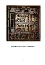
Страница 44: ...44 Fig 4 1 Model G 187 Receiver Top View Cover Removed...
Страница 45: ...45 Fig 4 2 Model G 187 Receiver Bottom View Covers Removed...
Страница 46: ...46 Fig 4 3 Model G 187 Receiver Rear View...
Страница 47: ...47 Fig 4 4 Model G 187 Receiver Panoramic Top View Cover Removed...
Страница 48: ...48 Fig 4 5 Model G 187 Receiver Panoramic Top View Left Side Cover Removed...
Страница 49: ...49 Fig 4 6 Model G 187 Receiver Panoramic Top View Right Side Cover Removed...
Страница 50: ...50 Fig 4 7 Model G 187 Receiver Panoramic Bottom View Covers Removed...
Страница 51: ...51 Fig 4 8 Model G 187 Receiver Panoramic Bottom View Left Side Covers Removed...
Страница 52: ...52 Fig 4 9 Model G 187 Receiver Panoramic Bottom View Right Side Covers Removed...
Страница 53: ...53 Table 4 2 Model G 187 Receiver Component Boards Lists...
Страница 54: ...54 Fig 4 10 Model G 187 Receiver Large Component Board...
Страница 56: ...56 Fig 4 14 Model G 187 Receiver Master Slave RF Tuners Top View...
Страница 57: ...57 Fig 4 15 Model G 187 Receiver Master Slave Tuners Bottom View Covers Removed...
Страница 58: ...58 Fig 4 16 Model G 187 Receiver Master Slave Tuners Panoramic Bottom View Covers Removed...
Страница 59: ...59 Fig 4 17 Model G 187 Receiver Master RF Tuner Bottom View Cover Removed...
Страница 60: ...60 Fig 4 18 Model G 187 Receiver Slave RF Tuner Bottom View Cover Removed...
Страница 67: ...67 Fig 5 1 Model G 187 Receiver Schematic Diagram Master RF Tuner...
Страница 68: ...68 Fig 5 2 Model G 187 Receiver Schematic Diagram Slave RF Tuner...
Страница 69: ...69 Fig 5 3 Model G 187 Receiver Schematic Diagram 21 4 Mc 200 Kc BW IF Strip Master and Slave Channels...
Страница 70: ...70 Fig 5 4 Model G 187 Receiver Schematic Diagram 2 5 Mc 40 Kc BW IF Nuvistor Strip Master and Slave Channels...
Страница 71: ...71 Fig 5 5 Model G 187 Receiver Schematic Diagram Main Chassis Circuits...
Страница 72: ...72 Fig 5 6 Model G 187 Receiver Schematic Diagram Mainframe...
Страница 73: ...73 Fig 5 7 Model G 187 Receiver Schematic Diagram Power Supply Circuits...
Страница 74: ...74 Fig 5 8 Model G 187 Receiver Schematic Diagram Various Details...