


24
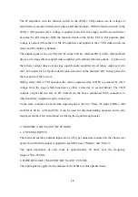
c. AUDIO AMPLIFIER
The output of V-103B is used to drive a two-stage resistance coupled audio amplifier. The
output amplifier drives an independent 600-ohm balanced output placed in the J-108 rear
socket.
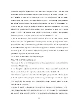
d. CARRIER OPERATED RELAY (COR)
The Carrier Operated Relay (COR) circuit is best described with the aid of the simplified
schematic of Fig. 2-3. This circuit provides carrier-on, carrier-off control of a panel light and
auxiliary equipment, provided such equipment is connected to the two available sets of relay
contacts through their terminating points on J-108, a socket on the chassis rear apron.
Fig. 2-3. Model G-187 Receiver COR Circuit, Simplified Schematic.
The relay is actuated when a carrier of adequate strength is received. When the carrier
disappears, the relay transfers to its unactuated position within 3 to 13 seconds. A chassis
rear-apron mounted COR DELAY ADJUST control (R-146) may be used to vary the delay
period of the carrier-off functioning within those limits of time.
Содержание G-187
Страница 7: ...7 Figure 1 1 Model G 187 Special Purpose Receiver Front View...
Страница 9: ...9 Table 1 2 Semiconductor and Tube Complement...
Страница 10: ...10 Table 1 2 Semiconductor and Tube Complement continued...
Страница 14: ...14 Fig 2 1 Block Diagram Model G 187 Receiver...
Страница 44: ...44 Fig 4 1 Model G 187 Receiver Top View Cover Removed...
Страница 45: ...45 Fig 4 2 Model G 187 Receiver Bottom View Covers Removed...
Страница 46: ...46 Fig 4 3 Model G 187 Receiver Rear View...
Страница 47: ...47 Fig 4 4 Model G 187 Receiver Panoramic Top View Cover Removed...
Страница 48: ...48 Fig 4 5 Model G 187 Receiver Panoramic Top View Left Side Cover Removed...
Страница 49: ...49 Fig 4 6 Model G 187 Receiver Panoramic Top View Right Side Cover Removed...
Страница 50: ...50 Fig 4 7 Model G 187 Receiver Panoramic Bottom View Covers Removed...
Страница 51: ...51 Fig 4 8 Model G 187 Receiver Panoramic Bottom View Left Side Covers Removed...
Страница 52: ...52 Fig 4 9 Model G 187 Receiver Panoramic Bottom View Right Side Covers Removed...
Страница 53: ...53 Table 4 2 Model G 187 Receiver Component Boards Lists...
Страница 54: ...54 Fig 4 10 Model G 187 Receiver Large Component Board...
Страница 56: ...56 Fig 4 14 Model G 187 Receiver Master Slave RF Tuners Top View...
Страница 57: ...57 Fig 4 15 Model G 187 Receiver Master Slave Tuners Bottom View Covers Removed...
Страница 58: ...58 Fig 4 16 Model G 187 Receiver Master Slave Tuners Panoramic Bottom View Covers Removed...
Страница 59: ...59 Fig 4 17 Model G 187 Receiver Master RF Tuner Bottom View Cover Removed...
Страница 60: ...60 Fig 4 18 Model G 187 Receiver Slave RF Tuner Bottom View Cover Removed...
Страница 67: ...67 Fig 5 1 Model G 187 Receiver Schematic Diagram Master RF Tuner...
Страница 68: ...68 Fig 5 2 Model G 187 Receiver Schematic Diagram Slave RF Tuner...
Страница 69: ...69 Fig 5 3 Model G 187 Receiver Schematic Diagram 21 4 Mc 200 Kc BW IF Strip Master and Slave Channels...
Страница 70: ...70 Fig 5 4 Model G 187 Receiver Schematic Diagram 2 5 Mc 40 Kc BW IF Nuvistor Strip Master and Slave Channels...
Страница 71: ...71 Fig 5 5 Model G 187 Receiver Schematic Diagram Main Chassis Circuits...
Страница 72: ...72 Fig 5 6 Model G 187 Receiver Schematic Diagram Mainframe...
Страница 73: ...73 Fig 5 7 Model G 187 Receiver Schematic Diagram Power Supply Circuits...
Страница 74: ...74 Fig 5 8 Model G 187 Receiver Schematic Diagram Various Details...