


37
(6) Increase the signal generator output to produce approximately the same value on the
VTVM as in (4) above.
(7) Adjust the secondary slug of T-507 for a maximum reading on the VTVM.
(8) Adjust the primary slug of T-507 for a maximum reading, keeping the signal generator
output adjusted for the same value on the VTVM as in (4) above. DO NOT readjust the
secondary for a maximum as this will result in improper alignment.
The second limiter transformer, T-507, has a 3.0 dB bandwidth large enough. The low circuit
Q’s and heavy coupling make visual alignment of this transformer desirable but not essential.
The procedure outlined above will produce less than 1.0 dB tilt in the response of this
transformer. Thus the slope is negligible over the 200 Kc. bandwidth.
c. Discriminator Alignment (CW Method).— In preparation for alignment of the
discriminator transformer, T-508, remove the 6AK5 (second limiter tube V-504), and note the
reading of the center frequency meter M-102. If it is off center, it should be centered by
means of the potentiometer R-118, located on the rear apron of the chassis. Difficulty in
readily securing an exact center reading is indicative of a defective 6AL5 tube (V-505), a
defective 12AU7A tube (V-101) or their associated components, and must be corrected
before proceeding further.
After this adjustment, replace V
-
504 and proceed as follows:
(1) Remove V-502.
(2) Set the signal generator to 21.4 Mc. and connect to pin 1 (control grid) of V-503.
(3) Connect a high-resistance DC voltmeter (VTVM) to the second limiter (V-504) grid
return.
(4) Set the signal generator output to produce 2 Volts on the VTVM.
(5) Connect the VTVM to the discriminator output lead.
(6) Tune the secondary of T-508 to zero output, then counterclockwise until the VTVM shows
a reading of 0.5 Volt.
(7) Tune the primary of T-508 to give a maximum reading on the VTVM.
(8) Retune the secondary to produce a zero (balance) reading on the VTVM.
Содержание G-187
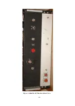
Страница 7: ...7 Figure 1 1 Model G 187 Special Purpose Receiver Front View...
Страница 9: ...9 Table 1 2 Semiconductor and Tube Complement...
Страница 10: ...10 Table 1 2 Semiconductor and Tube Complement continued...
Страница 14: ...14 Fig 2 1 Block Diagram Model G 187 Receiver...
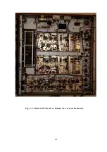
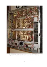
Страница 44: ...44 Fig 4 1 Model G 187 Receiver Top View Cover Removed...
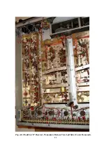
Страница 45: ...45 Fig 4 2 Model G 187 Receiver Bottom View Covers Removed...
Страница 46: ...46 Fig 4 3 Model G 187 Receiver Rear View...
Страница 47: ...47 Fig 4 4 Model G 187 Receiver Panoramic Top View Cover Removed...
Страница 48: ...48 Fig 4 5 Model G 187 Receiver Panoramic Top View Left Side Cover Removed...
Страница 49: ...49 Fig 4 6 Model G 187 Receiver Panoramic Top View Right Side Cover Removed...
Страница 50: ...50 Fig 4 7 Model G 187 Receiver Panoramic Bottom View Covers Removed...
Страница 51: ...51 Fig 4 8 Model G 187 Receiver Panoramic Bottom View Left Side Covers Removed...
Страница 52: ...52 Fig 4 9 Model G 187 Receiver Panoramic Bottom View Right Side Covers Removed...
Страница 53: ...53 Table 4 2 Model G 187 Receiver Component Boards Lists...
Страница 54: ...54 Fig 4 10 Model G 187 Receiver Large Component Board...
Страница 56: ...56 Fig 4 14 Model G 187 Receiver Master Slave RF Tuners Top View...
Страница 57: ...57 Fig 4 15 Model G 187 Receiver Master Slave Tuners Bottom View Covers Removed...
Страница 58: ...58 Fig 4 16 Model G 187 Receiver Master Slave Tuners Panoramic Bottom View Covers Removed...
Страница 59: ...59 Fig 4 17 Model G 187 Receiver Master RF Tuner Bottom View Cover Removed...
Страница 60: ...60 Fig 4 18 Model G 187 Receiver Slave RF Tuner Bottom View Cover Removed...
Страница 67: ...67 Fig 5 1 Model G 187 Receiver Schematic Diagram Master RF Tuner...
Страница 68: ...68 Fig 5 2 Model G 187 Receiver Schematic Diagram Slave RF Tuner...
Страница 69: ...69 Fig 5 3 Model G 187 Receiver Schematic Diagram 21 4 Mc 200 Kc BW IF Strip Master and Slave Channels...
Страница 70: ...70 Fig 5 4 Model G 187 Receiver Schematic Diagram 2 5 Mc 40 Kc BW IF Nuvistor Strip Master and Slave Channels...
Страница 71: ...71 Fig 5 5 Model G 187 Receiver Schematic Diagram Main Chassis Circuits...
Страница 72: ...72 Fig 5 6 Model G 187 Receiver Schematic Diagram Mainframe...
Страница 73: ...73 Fig 5 7 Model G 187 Receiver Schematic Diagram Power Supply Circuits...
Страница 74: ...74 Fig 5 8 Model G 187 Receiver Schematic Diagram Various Details...