


36
(6) Adjust C-220 for a 15% dip in the response.
(7) Repeat (5) above.
(8) Set dial to 250 Mc. and bend end inductors L-207 and L-209 to produce a
symmetrical
response centered at 250 Mc. Use 250 Mc. marker.
(9) Unsolder C-248 from the BNC test connector and resolder to the inductuner.
(10) Connect sweep generator to the antenna jack J-101 (or J-102 according to the situation).
NOTE: An accurate 50-ohm source can be achieved by using a 6
or 10 dB Ohm pad between
the sweep generator output and the receiver input.
(11) Set the dial to 70 Mc.
(12) Adjust C-243 for a symmetrical response.
(13) Set the dial to 250 Mc. and move the position of C-244 along the end portion of end
inductor L-204 to produce a symmetrical round-nose response.
5. IF ALIGNMENT—
(CW Method)
a. Introduction.- In the event that it should become necessary to align the IF strip, and a
suitable sweep generator and oscilloscope are not readily available, the following CW
alignment procedure is included. It is to be noted that alignment by the sweep method is more
efficient and effective than the CW method that follows, and, alignment by the sweep method
is more easily adaptable to trouble-shooting should the necessity arise. Therefore, if suitable
equipment is available, the sweep method of alignment should be used.
“Master” 200 Kc. IF Channel Alignment
b. Second Limiter Alignment.— (CW Method)
(1) Remove second IF amplifier V-502 from its socket.
(2) Set the signal generator to 21.4 Mc. and connect its output to the control grid (pin 1) of V-
503.
(3) Connect a high-resistance voltmeter (VTVM) to the grid return of V-504.
(4) Set the signal generator output to produce approvimately 2.0 Volts on the VTVM.
(5) Detune the primary slug of T-507 counterclockwise against the stop.
Содержание G-187
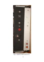
Страница 7: ...7 Figure 1 1 Model G 187 Special Purpose Receiver Front View...
Страница 9: ...9 Table 1 2 Semiconductor and Tube Complement...
Страница 10: ...10 Table 1 2 Semiconductor and Tube Complement continued...
Страница 14: ...14 Fig 2 1 Block Diagram Model G 187 Receiver...
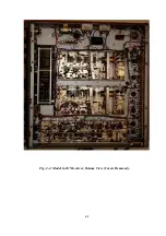
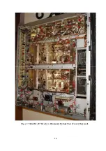
Страница 44: ...44 Fig 4 1 Model G 187 Receiver Top View Cover Removed...
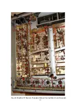
Страница 45: ...45 Fig 4 2 Model G 187 Receiver Bottom View Covers Removed...
Страница 46: ...46 Fig 4 3 Model G 187 Receiver Rear View...
Страница 47: ...47 Fig 4 4 Model G 187 Receiver Panoramic Top View Cover Removed...
Страница 48: ...48 Fig 4 5 Model G 187 Receiver Panoramic Top View Left Side Cover Removed...
Страница 49: ...49 Fig 4 6 Model G 187 Receiver Panoramic Top View Right Side Cover Removed...
Страница 50: ...50 Fig 4 7 Model G 187 Receiver Panoramic Bottom View Covers Removed...
Страница 51: ...51 Fig 4 8 Model G 187 Receiver Panoramic Bottom View Left Side Covers Removed...
Страница 52: ...52 Fig 4 9 Model G 187 Receiver Panoramic Bottom View Right Side Covers Removed...
Страница 53: ...53 Table 4 2 Model G 187 Receiver Component Boards Lists...
Страница 54: ...54 Fig 4 10 Model G 187 Receiver Large Component Board...
Страница 56: ...56 Fig 4 14 Model G 187 Receiver Master Slave RF Tuners Top View...
Страница 57: ...57 Fig 4 15 Model G 187 Receiver Master Slave Tuners Bottom View Covers Removed...
Страница 58: ...58 Fig 4 16 Model G 187 Receiver Master Slave Tuners Panoramic Bottom View Covers Removed...
Страница 59: ...59 Fig 4 17 Model G 187 Receiver Master RF Tuner Bottom View Cover Removed...
Страница 60: ...60 Fig 4 18 Model G 187 Receiver Slave RF Tuner Bottom View Cover Removed...
Страница 67: ...67 Fig 5 1 Model G 187 Receiver Schematic Diagram Master RF Tuner...
Страница 68: ...68 Fig 5 2 Model G 187 Receiver Schematic Diagram Slave RF Tuner...
Страница 69: ...69 Fig 5 3 Model G 187 Receiver Schematic Diagram 21 4 Mc 200 Kc BW IF Strip Master and Slave Channels...
Страница 70: ...70 Fig 5 4 Model G 187 Receiver Schematic Diagram 2 5 Mc 40 Kc BW IF Nuvistor Strip Master and Slave Channels...
Страница 71: ...71 Fig 5 5 Model G 187 Receiver Schematic Diagram Main Chassis Circuits...
Страница 72: ...72 Fig 5 6 Model G 187 Receiver Schematic Diagram Mainframe...
Страница 73: ...73 Fig 5 7 Model G 187 Receiver Schematic Diagram Power Supply Circuits...
Страница 74: ...74 Fig 5 8 Model G 187 Receiver Schematic Diagram Various Details...