


22
4. OTHER CIRCUITS
a. VIDEO
The output of the “Master” channel of the IF strips (200 or 40 Kc) drives one half of a
12AU7A direct-coupled video amplifier (V-101A). A zero center scale meter (M-102) is used
as a tuning indicator and is connected in a bridge circuit consisting of the video amplifier and
the other half of the 12AU7A (V-101B). A partial bypass of the cathode of the first video
amplifier extends the high frequency response. The output video amplifier is a 12AU7A tube
(V-102) connected as a direct-coupled cathode follower. A potentiometer (R-122) in series
with the cathode resistor of the output video amplifier provides the signal source to drive the
monitor audio amplifier, V-104.
b. SQUELCH
The squelch circuit is best described with the aid of the simplified schematic of Fig. 2-2.
V-103B (1/2 12AU7A) acts as a gated audio amplifier stage, while V-103A (1/2 12AU7A)
serves as a d-c amplifier and gate generator. The circuit is connected in such a manner that V-
103A has zero grid voltage when no signal is being received and has a negative signal applied
when a carrier is being received. The audio amplifier stage, V-103B, will pass an audio signal
when the d-c amplifier, V-103A, is nonconducting, and will not pass an audio signal when V-
103A is in a conducting condition. In this manner the audio circuit is disabled when no carrier
is being received. The carrier strength necessary to make the audio section operative is
adjusted by the threshold (squelch) control R-107.
The operation of this circuit is detailed in the following paragraph.
The DC amplifier tube, V-103A, is connected between the 150V supply and ground. The
fixed bias on this stage is adjusted by R-107. The audio section, V-103B, is connected
between the 250 volt supply and the 150 volt supply. The bias on this stage is the voltage drop
across the cathode resistor, R-131, plus the voltage drop, if any, in the plate load resistor, R-
129, in V-103A. Assuming no signal is being received, the grid of the DC amplifier tube is
zero, or at most has a very small negative voltage on it.
Содержание G-187
Страница 7: ...7 Figure 1 1 Model G 187 Special Purpose Receiver Front View...
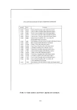
Страница 9: ...9 Table 1 2 Semiconductor and Tube Complement...
Страница 10: ...10 Table 1 2 Semiconductor and Tube Complement continued...
Страница 14: ...14 Fig 2 1 Block Diagram Model G 187 Receiver...
Страница 44: ...44 Fig 4 1 Model G 187 Receiver Top View Cover Removed...
Страница 45: ...45 Fig 4 2 Model G 187 Receiver Bottom View Covers Removed...
Страница 46: ...46 Fig 4 3 Model G 187 Receiver Rear View...
Страница 47: ...47 Fig 4 4 Model G 187 Receiver Panoramic Top View Cover Removed...
Страница 48: ...48 Fig 4 5 Model G 187 Receiver Panoramic Top View Left Side Cover Removed...
Страница 49: ...49 Fig 4 6 Model G 187 Receiver Panoramic Top View Right Side Cover Removed...
Страница 50: ...50 Fig 4 7 Model G 187 Receiver Panoramic Bottom View Covers Removed...
Страница 51: ...51 Fig 4 8 Model G 187 Receiver Panoramic Bottom View Left Side Covers Removed...
Страница 52: ...52 Fig 4 9 Model G 187 Receiver Panoramic Bottom View Right Side Covers Removed...
Страница 53: ...53 Table 4 2 Model G 187 Receiver Component Boards Lists...
Страница 54: ...54 Fig 4 10 Model G 187 Receiver Large Component Board...
Страница 56: ...56 Fig 4 14 Model G 187 Receiver Master Slave RF Tuners Top View...
Страница 57: ...57 Fig 4 15 Model G 187 Receiver Master Slave Tuners Bottom View Covers Removed...
Страница 58: ...58 Fig 4 16 Model G 187 Receiver Master Slave Tuners Panoramic Bottom View Covers Removed...
Страница 59: ...59 Fig 4 17 Model G 187 Receiver Master RF Tuner Bottom View Cover Removed...
Страница 60: ...60 Fig 4 18 Model G 187 Receiver Slave RF Tuner Bottom View Cover Removed...
Страница 67: ...67 Fig 5 1 Model G 187 Receiver Schematic Diagram Master RF Tuner...
Страница 68: ...68 Fig 5 2 Model G 187 Receiver Schematic Diagram Slave RF Tuner...
Страница 69: ...69 Fig 5 3 Model G 187 Receiver Schematic Diagram 21 4 Mc 200 Kc BW IF Strip Master and Slave Channels...
Страница 70: ...70 Fig 5 4 Model G 187 Receiver Schematic Diagram 2 5 Mc 40 Kc BW IF Nuvistor Strip Master and Slave Channels...
Страница 71: ...71 Fig 5 5 Model G 187 Receiver Schematic Diagram Main Chassis Circuits...
Страница 72: ...72 Fig 5 6 Model G 187 Receiver Schematic Diagram Mainframe...
Страница 73: ...73 Fig 5 7 Model G 187 Receiver Schematic Diagram Power Supply Circuits...
Страница 74: ...74 Fig 5 8 Model G 187 Receiver Schematic Diagram Various Details...