


4-27
BUS PROTOCOL
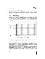
Three transactions are issued in clocks T1, T4, and T7. None of these transactions have write
data to transfer as indicated by the REQa0# signal.
The Snoop Phase for each transaction indicates that no implicit writeback data will be trans-
ferred and the response agent indicated by the address will provide the transaction response and
the read data if there is any.
Because the transactions have no write or implicit writeback data, the TRDY# signal is not
asserted.
The rcnt indicates that the In-order Queue is empty. The ADS# for transaction 1 is driven in T1.
The snoop results for transaction 1 are driven four clocks later in T5 (observed in T6). Note that
the Response and Data Phases for transaction n-1 have to be complete before the response for
transaction n can be driven. Since transaction 1 is at the top of the IOQ and DBSY# is inactive
in T6, RS[2:0]# can be driven for transaction 1 in T7, two clocks after the snoop results are driv-
en. Transaction 1 is removed from the IOQ after T8, and transaction 2 is now at the top of the
IOQ. The rcnt is not decremented in T9 because transaction 3 was issued in the same clock that
transaction 1 received its response.
Transaction 2 is issued to the bus in T4 (three clocks after Transaction 1). The snoop results for
transaction 2 are driven four clocks later in T8. Transaction 2 is at the top of the IOQ. RS[2:0]#
for transaction 2 is driven two clocks later in T10 because DBSY# and RS[2:0]# were sampled
deasserted in T9.
The response for transaction 3 cannot be driven two clocks after the snoop results are driven in
T11 because DBSY# is asserted in T11. DBSY# is sampled deasserted in T13 and RS[2:0]# for
transaction 3 is driven in T14.
The response driven for each of these transactions is the Normal Data Response.
Figure 4-14. RS[2:0]# Activation with no TRDY#
CLK
DBSY#
TRDY#
HITM#
RS[2:0]#
1
2
3
4
5
6
7
8
9
10
11
12
13
14
15
16
ADS#
REQ0#
1
2
1
{rcnt}
0
0
1
1
1
2
2
2
2
2
2
1
1
1
1
0
3
2
3
Содержание Pentium Pro Family
Страница 17: ...1 Component Introduction ...
Страница 26: ...2 Pentium Pro Processor Architecture Overview ...
Страница 27: ......
Страница 36: ...3 Bus Overview ...
Страница 62: ...4 Bus Protocol ...
Страница 105: ...5 Bus Transactions and Operations ...
Страница 126: ...6 Range Registers ...
Страница 131: ...7 Cache Protocol ...
Страница 135: ...8 Data Integrity ...
Страница 148: ...9 Configuration ...
Страница 161: ...10 Pentium Pro Processor Test Access Port TAP ...
Страница 172: ...11 Electrical Specifications ...
Страница 201: ...12 GTL Interface Specification ...
Страница 229: ...13 3 3V Tolerant Signal Quality Specifications ...
Страница 233: ...14 Thermal Specifications ...
Страница 239: ...15 Mechanical Specifications ...
Страница 241: ...15 2 MECHANICAL SPECIFICATIONS s Figure 15 1 Package Dimensions Bottom View ...
Страница 252: ...16 Tools ...
Страница 260: ...16 8 TOOLS Figure 16 4 Generic MP System Layout for Debug Port Connection ...
Страница 264: ...17 OverDrive Processor Socket Specification ...
Страница 290: ...A Signals Reference ...
Страница 320: ...Index ...
Страница 328: ......