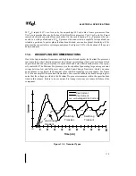


11-17
ELECTRICAL SPECIFICATIONS
11.14. GTL+ BUS SPECIFICATIONS
The GTL+ bus must be routed in a daisy-chain fashion with termination resistors at each
end of every signal trace. These termination resistors are placed between the ends of the signal
trace and the VTT voltage supply and generally are chosen to approximate the board impedance.
The valid high and low levels are determined by the input buffers using a reference voltage
called VREF. Table 11-8 lists the nominal specifications for the GTL+ termination voltage
(VTT) and the GTL+ reference voltage (VREF). It is important that the printed circuit board
impedance be specified and held to a
±
20% tolerance, and that the intrinsic trace capacitance
for the GTL+ signal group traces is known. For more details on GTL+, See Chapter 12,
GTL+ Interface Specification.
NOTE:
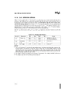
1. VREF should be created from VTT by a voltage divider of 1% resistors.
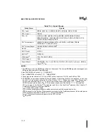
NOTES:
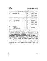
1. Table 11-7 applies to the 3.3V tolerant, APIC, and JTAG signal groups.
2. Parameter measured at 4 mA (for use with TTL inputs).
3. Parameter guaranteed by design at 100uA (for use with CMOS inputs).
4. (0
≤
Vpin
≤
VccP).
5. Total of I/O buffer, package parasitics and 0.5pF for a socket. Capacitance values are guaranteed by
design.
VIH
Input High Voltage
2.0
3.6
V
VOL
Output Low Voltage
0.4
0.2
V
V
2
3
VOH
Output High Voltage
N/A
N/A
V
All Outputs are Open-Drain
IOL
Output Low Current
24
mA
IL
Input Leakage Current
± 100
µ
A
4
CTOL
3.3V Tol. Pin Capacitance
10
pF
Except BCLK, TCK 5
CCLK
BCLK Input Capacitance
9
pF
5
CTCK
TCK Input Capacitance
8
pF
5
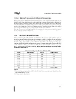
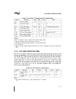
Table 11-8. GTL+ Bus D.C. Specifications
Symbol
Parameter
Min
Typical
Max
Units
Notes
VTT
Bus Termination
Voltage
1.35
1.5
1.65
V
± 10%
VREF
Input Reference
Voltage
2/3 VTT - 2%
2/3 VTT
2/3 VTT + 2%
V
± 2% 1
Table 11-7. Non-GTL+ 1 Signal Groups D.C. Specifications
Symbol
Parameter
Min
Max
Unit
Notes
Содержание Pentium Pro Family
Страница 17: ...1 Component Introduction ...
Страница 26: ...2 Pentium Pro Processor Architecture Overview ...
Страница 27: ......
Страница 36: ...3 Bus Overview ...
Страница 62: ...4 Bus Protocol ...
Страница 105: ...5 Bus Transactions and Operations ...
Страница 126: ...6 Range Registers ...
Страница 131: ...7 Cache Protocol ...
Страница 135: ...8 Data Integrity ...
Страница 148: ...9 Configuration ...
Страница 161: ...10 Pentium Pro Processor Test Access Port TAP ...
Страница 172: ...11 Electrical Specifications ...
Страница 201: ...12 GTL Interface Specification ...
Страница 229: ...13 3 3V Tolerant Signal Quality Specifications ...
Страница 233: ...14 Thermal Specifications ...
Страница 239: ...15 Mechanical Specifications ...
Страница 241: ...15 2 MECHANICAL SPECIFICATIONS s Figure 15 1 Package Dimensions Bottom View ...
Страница 252: ...16 Tools ...
Страница 260: ...16 8 TOOLS Figure 16 4 Generic MP System Layout for Debug Port Connection ...
Страница 264: ...17 OverDrive Processor Socket Specification ...
Страница 290: ...A Signals Reference ...
Страница 320: ...Index ...
Страница 328: ......