


3-9
BUS OVERVIEW
3.3.4.1.
LINE TRANSFERS
A line transfer reads or writes a cache line, the unit of caching in a Pentium Pro processor sys-
tem. On the Pentium Pro processor this is 32 bytes aligned on a 32-byte boundary. While a line
is always aligned on a 32-byte boundary, a line transfer need not begin on that boundary. For a
line transfer on the Pentium Pro processor, A[35:3]# carry the upper 33 bits of a 36-bit physical
address. Address bits A[4:3]# determine the transfer order, called burst order. A line is trans-
ferred in four eight-byte chunks, each of which can be identified by address bits 4:3. The chunk
size is 64-bits. Table 3-1 specifies the transfer order used for a 32-byte line, based on address
bits A[4:3]# specified in the transaction’s Request Phase.
Note that the requested read data is always transferred first. Unlike the Pentium processor, which
always transfers writeback data address 0 first, the Pentium Pro processor transfers writeback
data requested address first.
3.3.4.2.
PART LINE ALIGNED TRANSFERS
A part-line aligned transfer moves a quantity of data smaller than a cache line but an even mul-
tiple of the chunk size between a bus agent and memory using the burst order. A part-line trans-
fer affects no more than one line in a cache.
A 16-byte transfer on a 64-bit data bus with a 32-byte cache line size is a part-line transfer, where
a chunk is eight bytes aligned on an eight-byte boundary. All chunks in the span of a part-line
transfer are moved across the data bus. Address bits A[4:3]# determines the transfer order for
the included chunks, using the burst order specified in Table 3-1 for line transfers.
A 16-byte aligned transfer requires two data transfer clocks on a 64-bit bus. Note that the Pen-
tium Pro processor will not issue 16-byte transactions.
3.3.4.3.
PARTIAL TRANSFERS
On a 64-bit data bus, a partial transfer moves from 0-8 bytes within an aligned 8-byte span to or
from a memory or I/O address. The byte enable signals, BE[7:0]#, select which bytes in the span
are transferred.
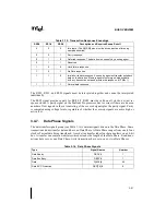
Table 3-1. Burst Order Used For Pentium
®
Pro Processor Bus Line Transfers
A[4:3]#
(binary)
Requested
Address
(hex)
1st Address
Transferred
(hex)
2nd Address
Transferred
(hex)
3rd Address
Transferred
(hex)
4th Address
Transferred
(hex)
00
0
0
8
10
18
01
8
8
0
18
10
10
10
10
18
0
8
11
18
18
10
8
0
Содержание Pentium Pro Family
Страница 17: ...1 Component Introduction ...
Страница 26: ...2 Pentium Pro Processor Architecture Overview ...
Страница 27: ......
Страница 36: ...3 Bus Overview ...
Страница 62: ...4 Bus Protocol ...
Страница 105: ...5 Bus Transactions and Operations ...
Страница 126: ...6 Range Registers ...
Страница 131: ...7 Cache Protocol ...
Страница 135: ...8 Data Integrity ...
Страница 148: ...9 Configuration ...
Страница 161: ...10 Pentium Pro Processor Test Access Port TAP ...
Страница 172: ...11 Electrical Specifications ...
Страница 201: ...12 GTL Interface Specification ...
Страница 229: ...13 3 3V Tolerant Signal Quality Specifications ...
Страница 233: ...14 Thermal Specifications ...
Страница 239: ...15 Mechanical Specifications ...
Страница 241: ...15 2 MECHANICAL SPECIFICATIONS s Figure 15 1 Package Dimensions Bottom View ...
Страница 252: ...16 Tools ...
Страница 260: ...16 8 TOOLS Figure 16 4 Generic MP System Layout for Debug Port Connection ...
Страница 264: ...17 OverDrive Processor Socket Specification ...
Страница 290: ...A Signals Reference ...
Страница 320: ...Index ...
Страница 328: ......