Additional information
27 of 31
Revision 4.0
2021-10-11
Recommendations for board assembly of Infineon transistor outline
type packages
Inspection
6.2
X-ray solder joint inspection
Automated X-ray inspection (AXI) systems are appropriate for efficient inline control of component parts that
cannot be inspected properly by optical systems (such as exposed pads). AXI systems are available as 2D and
3D solutions. They usually consist of an X-ray camera and the hardware and software needed for inspection,
controlling, analyzing, and data transferring routines. These reliable systems enable the user to detect
soldering defects such as poor soldering, bridging, voiding, and missing parts. However, other defects such as
broken solder joints are not easily detectable by X-ray.
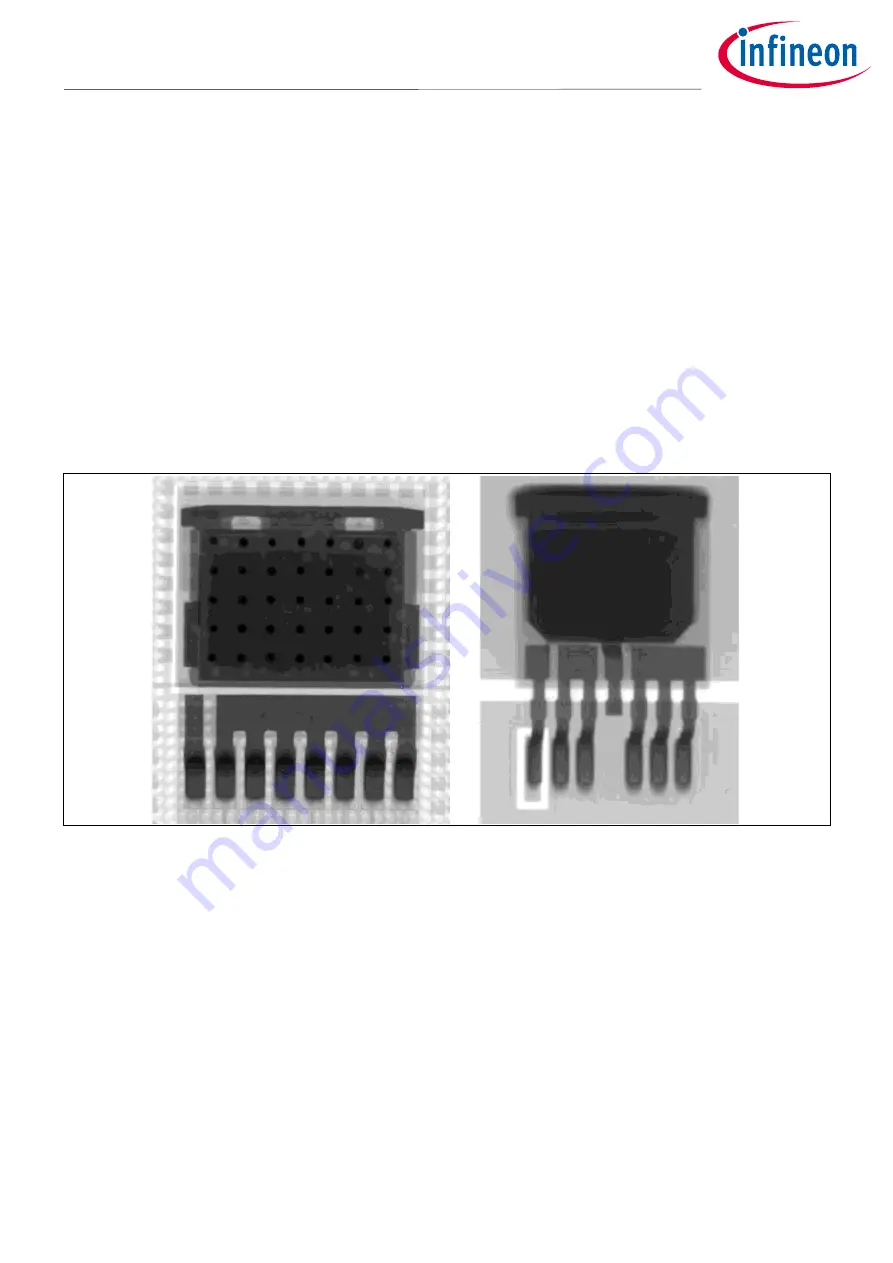
shows typical X-ray photographs of HSOG-8 and TO263-7 SMD components. The top and inner layers
of the boards as well as vias in the pad are visible. Large exposed pads may tend to increased voiding because
they do not provide a sufficient ratio between volume and surface necessary for proper outgassing of the
organic paste compounds during reflow. Generally, the extent of voiding depends on the board pad size, the via
and stencil layout, the solder paste, and the reflow profile. For thermal evaluations, the entire thermal path
must be considered as well as all boundary conditions such as the application environment or the electrical use
of the component
Figure 21
Typical X-ray image of a soldered HSOG-8 (left) and of a TO263-7 SMD package (right).


