background image


Additional information 

19 of 31 

Revision 4.0  


2021-10-11 


Recommendations for board assembly of Infineon transistor outline 
type packages 


Mounting of through-hole devices 


4.2


Component placement of THD 

THDs are inserted either with special automatic equipment or manually. During this insertion, special care has 
to be taken that excessive deformation or violent bending is avoided. The diameter of the drill holes in the PCB 
has to be appropriate for the tolerances of component leads, drill hole position placement accuracy, and 
properties of the solder alloy used. 

4.3


Heat sink mounting 

For special packages with high power dissipation, heat sinks can be mounted before or after soldering the 
leads. 

Insulating material 

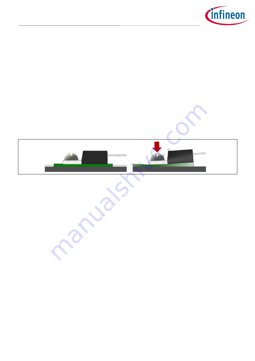
Commonly used insulating materials are mica and rubber. Mica is much harder than rubber. For softer 
materials, the mounting torque in particular needs to be controlled very carefully in order to avoid high 
mechanical stress and damage to the package as shown i

Figure 12

. 


Figure 12


Schematic view of the influence of the insulating material (left mica, right rubber) on the 
generation of mechanical stress. 

Thermal grease 

A specific amount of grease must be applied. The amount should be determined during customer process 
evaluation. When the amount is correct, a very small amount of grease should appear around the perimeter of 
each surface as the assembly is slowly torqued to the recommended value. Examination of a demounted 
assembly should reveal even wetting across each surface. 

Heat sink requirements 

The contact areas of the package and the heat sink must be free of any particles and damage as well as any 
other contamination. The following surface conditions are recommended: 

Heat sink roughness    

R

Z

 ≤ 10 µm 

Heat sink flatness  


≤ 10 µm (reference length 15 mm) 

Attachment holes 

Drill holes for heat sink screw mounting should be as small as possible. Using drill holes that are too big will 
reduce the effectiveness of the heat sink. 

The flatness and effectiveness of the heat sink will also be reduced by intrusions and/or burrs around the hole. 
These are caused by the punching or drilling process and should be less than the specified heat sink roughness 
and flatness. 

If intrusions or large drill holes are unavoidable, a fitting square washer should be used to get a good and flat 
contact between heat sink and package. 

Содержание PG-TO220

Страница 1: ...rmation Please read the Important Notice and Warnings at the end of this document Revision 4 0 www infineon com page 1 of 31 2021 10 11 Recommendations for board assembly of Infineon transistor outlin...

Страница 2: ...10 2 1 Routing 10 2 2 Pad design 10 2 3 Via in pad design 11 3 Mounting of surface mount devices 13 3 1 Solder paste stencil 13 3 2 Solder paste 13 3 3 Component placement of SMD 14 3 4 Reflow solderi...

Страница 3: ...ng IGBT insulated gate bipolar transistor I O input output K W Kelvin per Watts MOSFET metal oxide semiconductor field effect transistor MSL moisture sensitivity level NSMD non solder mask defined PG...

Страница 4: ...y this may require certain pre mount processing steps The heat sink of THD package can either be mounted on the board or can be equipped with an additional heatspreader The packages are optimized for...

Страница 5: ...ckage versions with screw mounting hole and without it featuring an increased heatsink area Plus version Some packages feature leads with extended or reduced length Long lead and Short lead versions I...

Страница 6: ...dling guidelines Semiconductor devices are sensitive to excessive electrostatic discharge ESD moisture mechanical handling and contamination Therefore they require specific precautionary measures to e...

Страница 7: ...showing the inner setup of a TO SMD package Figure 5 Schematic showing the inner setup of a TO THT package Thermal performance The overall thermal performance of a package with a heat sink is charact...

Страница 8: ...isolated from its mounting surface The isolation material has a relatively high thermal resistance which raises junction operating temperatures For further information about thermal performance please...

Страница 9: ...neon transistor outline type packages Package description Termination plating Infineon TO SMD and HSOG packages with gullwing leads feature a matte tin Sn surface finish that is applied to the base me...

Страница 10: ...solder mask defined SMD or non solder mask defined NSMD Specific pad dimensions Pad finish also called metallization or final finish Via layout and technology For optimal heat dissipation in high curr...

Страница 11: ...resistance of the entire assembly set up Thermal and electrical analysis and or testing together with a proper board assembly design procedure are recommended to determine the optimal number of vias...

Страница 12: ...tor outline type packages Printed circuit board For further information about vias in pad please refer to the General Recommendations for Board Assembly of Infineon Packages document that is available...

Страница 13: ...lder paste volume in apertures larger than approximately 5 mm may be scooped out depending on the specific squeegee pressure and rigidity Such apertures are necessary for many die pad prints and shoul...

Страница 14: ...ble solder joints the components have to be placed accurately depending on their geometry An automated pick and place machine is recommended to obtain reliable solder joints Component placement accura...

Страница 15: ...he reflow profile i e where the solder is liquid the components are only held in place by wetting forces from the molten solder Gravity acting in the opposite direction will elongate the solder joints...

Страница 16: ...art reliability Lead cutting The leads of THDs can be cut before mounting or after mounting and soldering In case of cutting after soldering the leads are embedded in the solder joint Severe mechanica...

Страница 17: ...lead forming as this has the potential to mechanically damage the package particularly at the metal to plastic interface In case of a package containing an isolated backside e g FullPAK packages TO24...

Страница 18: ...orrect lead clamping and bending of THD packages right Figure 11 Parameters for recommended minimum clamping distance and radius for lead bending Manual bending Manual bending is generally not recomme...

Страница 19: ...right rubber on the generation of mechanical stress Thermal grease A specific amount of grease must be applied The amount should be determined during customer process evaluation When the amount is co...

Страница 20: ...ndependent from the number of leads of the respective package Package Insulator Thermal grease Insulating bushing Washer TO220 Yes No Yes Yes TO220 FullPAK No Yes No Yes TO247 Yes No Yes Yes TO247 Adv...

Страница 21: ...t sink assembly with screw mounting Improper mounting can damage a die Molding compound can delaminate due to external mechanical stress e g mounting on warped heat sink a shown in Figure 15 Figure 15...

Страница 22: ...al Heat sink clip mounting The clip mounting method has become popular because it is simple and reliable The process is fast and appropriate for mass production assembly The screw mounting is applied...

Страница 23: ...ds and body and inside the package is steeper compared to reflow soldering The heat resistance of wave solderable TO THD is tested according to JESD22 B106 and IEC 60068 2 20 typically 260 C for 10 s...

Страница 24: ...If extended contact and heating times are unavoidable the resulting temperature on various leads near the package body should be measured and must not exceed the temperature and duration experienced d...

Страница 25: ...clean flux is recommended whose residues usually do not have to be removed after the soldering process In case the solder joints have to be cleaned the cleaning method e g ultrasonic spray or vapor cl...

Страница 26: ...joints of the outer gullwing shaped terminations with conventional automated optical inspection AOI systems is a standard procedure According to IPC A 610 the top side of a gullwing lead as well as t...

Страница 27: ...and missing parts However other defects such as broken solder joints are not easily detectable by X ray Figure 21 shows typical X ray photographs of HSOG 8 and TO263 7 SMD components The top and inne...

Страница 28: ...the component prior to rework might be necessary A proper drying procedure for SMD packages is described in the international J STD 033 standard 6 Please also refer to the recommendations of your PCB...

Страница 29: ...and JEDEC Solid State Technology Association Committee EIA IPC JEDEC J STD 002 Solderability Tests for Component Leads Terminations Lugs Terminals and Wires 5 JEDEC Solid State Technology Association...

Страница 30: ...11 Recommendations for board assembly of Infineon transistor outline type packages Revision history Revision history Page or reference Major changes since the last revision Entire document Transfer to...

Страница 31: ...property rights of any third party with respect to any and all information given in this application note The data contained in this document is exclusively intended for technically trained staff It i...

Отзывы: