3. Processor Bus Interface
87
PowerSpan II User Manual
80A1010_MA001_09
Integrated Device Technology
www.idt.com
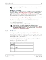
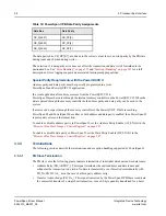
Master-based Decode Mode
The PB Slave Interface supports Master-based decode mode when the internal PowerSpan II processor
bus arbiter is enabled (see
“Processor Bus Arbitration” on page 141
) and the Master Decode Enable
(MD_EN) bit is set in the
“Processor Bus Slave Image x Control Register” on page 287
. When
Master-based decode is enabled, a PB slave image only claims a transaction decoded for its specified
physical address space if it originates from specific processor bus master or masters.
External bus masters are selected for a specific target by setting one or more of the M1 to M3 bits in the
“Processor Bus Slave Image x Translation Address Register” on page 292
The PB slave image only claims a transaction when all of the following conditions are met:
•
the address matches the slave image
•
the transaction codes are supported
•
Mx is set and the identified master is requesting a transaction
3.3.1.2
Transfer Types
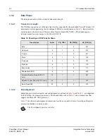
The PB Slave only claims processor bus transactions with specific transfer types. The supported
transfer types consist of address only, read, and write. They are defined in
All reads are treated as delayed reads and can be single cycle, extended or bursts. All writes are treated
as posted writes and can be single cycle, extended or bursts. PowerSpan II handles address only cycles
by asserting PB_AACK_
—
no data transfer occurs.
Address only transfer types are claimed to ensure PowerSpan II does not negatively impact cache
control, reservation, or ordering transactions on the processor bus.
Register and PCI I/O space accesses requires I to be set to 1 because PowerSpan II does not
accept burst transactions to these resources.
PowerSpan II behavior is undefined if more than one identically programmed, or
overlapping, slave image claims a transaction. For example, if two slave image have the same
base address and size, then they must have unique master bits set in the
Image x Translation Address Register” on page 292
Table 13: PowerSpan II PB Slave Transfer Types
TT[0:4]
Name
Address Only
00000
Clean Block
00100
Flush Block
01000
Sync Block
01100
Kill Block
Содержание PowerSpan II
Страница 8: ...Contents 8 PowerSpan II User Manual 80A1010_MA001_09 Integrated Device Technology www idt com ...
Страница 14: ...List of Tables 14 PowerSpan II User Manual 80A1010_MA001_09 Integrated Device Technology www idt com ...
Страница 18: ...About this Document 18 PowerSpan II User Manual 80A1010_MA001_09 Integrated Device Technology www idt com ...
Страница 82: ...2 PCI Interface 82 PowerSpan II User Manual 80A1010_MA001_09 Integrated Device Technology www idt com ...
Страница 112: ...3 Processor Bus Interface 112 PowerSpan II User Manual 80A1010_MA001_09 Integrated Device Technology www idt com ...
Страница 156: ...7 Interrupt Handling 156 PowerSpan II User Manual 80A1010_MA001_09 Integrated Device Technology www idt com ...
Страница 380: ...12 Register Descriptions 380 PowerSpan II User Manual 80A1010_MA001_09 Integrated Device Technology www idt com ...
Страница 394: ...14 Package Information 394 PowerSpan II User Manual 80A1010_MA001_09 Integrated Device Technology www idt com ...
Страница 414: ...15 AC Timing 414 PowerSpan II User Manual 80A1010_MA001_09 Integrated Device Technology www idt com ...
Страница 416: ...16 Ordering Information 416 PowerSpan II User Manual 80A1010_MA001_09 Integrated Device Technology www idt com ...
Страница 420: ...A Hardware Implementation 420 PowerSpan II User Manual 80A1010_MA001_09 Integrated Device Technology www idt com ...
Страница 428: ...B Typical Applications 428 PowerSpan II User Manual 80A1010_MA001_09 Integrated Device Technology www idt com ...
Страница 432: ...Glossary 432 PowerSpan II User Manual 80A1010_MA001_09 Integrated Device Technology www idt com ...


