3. Processor Bus Interface
97
PowerSpan II User Manual
80A1010_MA001_09
Integrated Device Technology
www.idt.com
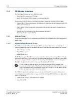
Discard Timer
Each PB slave image has a discard timer. If an external master does not claim data within 2
15
clocks
after data is read from the destination bus, the Delayed Read Request latch is de-allocated. This
prevents deadlock conditions. Read buffer contents are flushed but there is no error recorded and no
interrupts are generated.
Posted Writes
Posted writes have dedicated line buffers and are treated independently of reads. A write to an image
does not invalidate the contents of the read line buffer currently in use.
Address Retry Disabled
The PB Slave supports a single read at a time when ARTRY_EN is disabled. ARTRY_EN is disabled
by setting the bit to 0. The PB slave acknowledges the address tenure with the PB_AACK_ signal and
captures the address in the Delayed Read latch. However, when ARTRY_EN is disabled, the PB slave
does not acknowledge the data transfer until the Read Amount (RD_AMT) field in the
Slave Image x Control Register” on page 287
is read. The Delayed Read Request latch is de-allocated
when the external processor bus master completes the transaction.
PRKEEP has no affect when PKEEP is set to 1 and ARTRY_EN is disabled. A maximum of 32 bytes
can be programmed in the RD_AMT field.
3.3.2.5
Writes
All writes are posted and are buffered separately from read data. The transaction length of the PB write
is directly translated to the PCI bus with no address phase deletion. For example, a single cycle write
on the PB results in a single cycle write on the PCI bus.
3.3.2.6
Data Parity
Data parity is enabled by setting the Data Parity Enable (DP_EN) bit in the
Miscellaneous Control and Status Register” on page 304
. Even parity or odd parity is enabled by
setting the Parity (PARITY) bit in the same register.
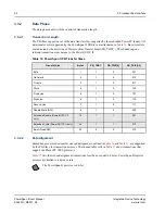
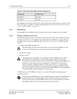
Parity generation and checking is provided for each byte of the data bus and for each data beat of the
data tenure. Data parity bit assignments are as defined in Table 19.
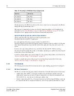
Table 19: PowerSpan II PB Data Parity Assignments
Data Bus
Data Parity
PB_D[0:7]
PB_DP[0]
PB_D[8:15]
PB_DP[1]
PB_D[16:23]
PB_DP[2]
PB_D[24:31]
PB_DP[3]
PB_D[32:39]
PB_DP[4]
Содержание PowerSpan II
Страница 8: ...Contents 8 PowerSpan II User Manual 80A1010_MA001_09 Integrated Device Technology www idt com ...
Страница 14: ...List of Tables 14 PowerSpan II User Manual 80A1010_MA001_09 Integrated Device Technology www idt com ...
Страница 18: ...About this Document 18 PowerSpan II User Manual 80A1010_MA001_09 Integrated Device Technology www idt com ...
Страница 82: ...2 PCI Interface 82 PowerSpan II User Manual 80A1010_MA001_09 Integrated Device Technology www idt com ...
Страница 112: ...3 Processor Bus Interface 112 PowerSpan II User Manual 80A1010_MA001_09 Integrated Device Technology www idt com ...
Страница 156: ...7 Interrupt Handling 156 PowerSpan II User Manual 80A1010_MA001_09 Integrated Device Technology www idt com ...
Страница 380: ...12 Register Descriptions 380 PowerSpan II User Manual 80A1010_MA001_09 Integrated Device Technology www idt com ...
Страница 394: ...14 Package Information 394 PowerSpan II User Manual 80A1010_MA001_09 Integrated Device Technology www idt com ...
Страница 414: ...15 AC Timing 414 PowerSpan II User Manual 80A1010_MA001_09 Integrated Device Technology www idt com ...
Страница 416: ...16 Ordering Information 416 PowerSpan II User Manual 80A1010_MA001_09 Integrated Device Technology www idt com ...
Страница 420: ...A Hardware Implementation 420 PowerSpan II User Manual 80A1010_MA001_09 Integrated Device Technology www idt com ...
Страница 428: ...B Typical Applications 428 PowerSpan II User Manual 80A1010_MA001_09 Integrated Device Technology www idt com ...
Страница 432: ...Glossary 432 PowerSpan II User Manual 80A1010_MA001_09 Integrated Device Technology www idt com ...

