APEX
™
Exciter Incorporating FLO
™
Technology
Navigating the LCD Display Screens
Details of the Exciter Status Screens
Page: 3-10
888-2604-001
03/08/07
WARNING: Disconnect primary power prior to servicing.
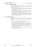
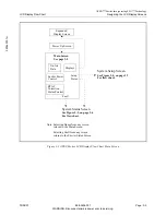
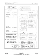
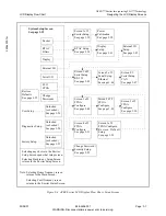
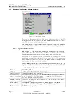
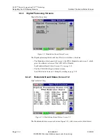
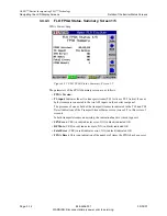
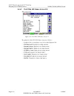
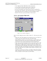
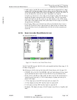
The Adaptive Processing Board status screen is shown in Figure 3-7, with screen entries
listed below.
• 3.3 Vdc: This is the output of the 3.3 V dc to dc converter.
• 5 Vdc: This is the board input voltage, which comes from the controller board.
• AP 3.3 Vdc supply is derived from the 3.3 Vdc supply through an FET switch. This
voltage is switched off if the 1.9 Vdc AP supply faults.
• AP 1.9 Vdc: This is the output from the AP DSP core supply dc to dc converter.
• NL 3.3 Vdc supply is derived from the 3.3 Vdc supply through an FET switch. This
voltage is switched off if the 1.8 Vdc NL supply faults.
• NL 1.8 Vdc NL DSP core power supply.
• PLL Lock: (Ok or FAULT) This is the lock status of a PLL on the adaptive corrector
board. It locks the 22.2, and 44.4 MHz clocks to the 11.1 MHz clock from the FPGA
Modulator board.
• EEPROM: (Ok or FAULT) The EEPROM is the local board memory. It stores board
specific information such as board revision, AP CPLD revision, DSP revision, and
other local data.
• ADC Over Range: (OK or FAULT) Fault = One or more input RF voltage samples to
the ADC (analog to digital converter) exceeded maximum allowable level.
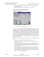
Each of the feedbacks listed below has a bar graph. The yellow (upper) bar indicates
average power level and the blue (lower) bar indicates peak level. The presence of an RF
sample which is within the correct power range (-30 to 0 dBm) is indicated when both bars
are within the center range of the window. The bar graphs are not calibrated to the input
power level. If any input sample is outside the allowable power range window, the bars for
that input will be at an extreme end of the window and that input will be faulted.
• HPF Feedback: (OK or FAULT)
This is the RF sample taken after the high power filter.
• PA feedback: (OK or FAULT)
This is the RF sample taken after the power amplifier but before the high power filter.
Note
The maximum input level for the three feedbacks mentioned above
should not exceed 0 dBm. Excessive input levels will cause faults for
the ADC and feedback inputs and can also cause crosstalk between in-
puts and/or damage to the exciter. +20 dBm is the damage level
• NL CPLD: (Ok or FAULT) This is the health status of the NL CPLD in the Adaptive
Precorrector board.
• Board Rev: This is the board revision for the Adaptive Precorrector board.
• AP CPLD Rev: This is the revision level of the AP CPLD in the Adaptive Precorrec-
tor board.
• AP DSP Rev: This is the revision level of the AP DSP (digital signal processor) soft-
ware in the Adaptive Precorrector board.
• NL DSP Rev: This is the revision level of the NL DSP (digital signal processor) soft-
ware in the Adaptive Precorrector board.

