
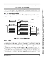
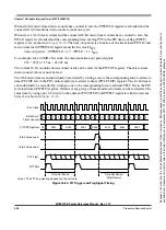


Chapter 19 Pulse-Width Modulator (S12PWM8B8CV1)
MC9S12XE-Family Reference Manual , Rev. 1.19
694
Freescale Semiconductor
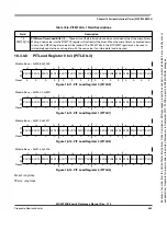
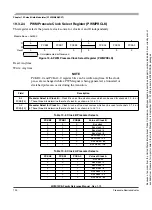
with the PWM and their relative offset from the base address. The register detail description follows the
order they appear in the register map.
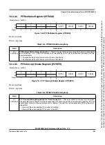
Reserved bits within a register will always read as 0 and the write will be unimplemented. Unimplemented
functions are indicated by shading the bit. .
NOTE
Register Address = Base A Address Offset, where the Base Address
is defined at the MCU level and the Address Offset is defined at the module
level.
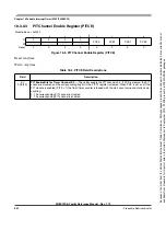
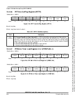
19.3.2
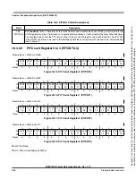
Register Descriptions
This section describes in detail all the registers and register bits in the PWM module.
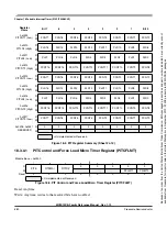
Register
Name
Bit 7
6
5
4
3
2
1
Bit 0
0x0000
PWME
R
PWME7
PWME6
PWME5
PWME4
PWME3
PWME2
PWME1
PWME0
W
0x0001
PWMPOL
R
PPOL7
PPOL6
PPOL5
PPOL4
PPOL3
PPOL2
PPOL1
PPOL0
W
0x0002
PWMCLK
R
PCLK7
PCLKL6
PCLK5
PCLK4
PCLK3
PCLK2
PCLK1
PCLK0
W
0x0003
PWMPRCLK
R
0
PCKB2
PCKB1
PCKB0
0
PCKA2
PCKA1
PCKA0
W
0x0004
PWMCAE
R
CAE7
CAE6
CAE5
CAE4
CAE3
CAE2
CAE1
CAE0
W
0x0005
PWMCTL
R
CON67
CON45
CON23
CON01
PSWAI
PFRZ
0
0
W
0x0006
PWMTST
(1)
R
0
0
0
0
0
0
0
0
W
0x0007
PWMPRSC
R
0
0
0
0
0
0
0
0
W
0x0008
PWMSCLA
R
Bit 7
6
5
4
3
2
1
Bit 0
W
0x0009
PWMSCLB
R
Bit 7
6
5
4
3
2
1
Bit 0
W
= Unimplemented or Reserved
Figure 19-2. PWM Register Summary (Sheet 1 of 3)
Because
of
an
order
from
the
United
States
International
Trade
Commission,
BGA-packaged
product
lines
and
part
numbers
indicated
here
currently
are
not
available
from
Freescale
for
import
or
sale
in
the
United
States
prior
to
September
2010:
S12XE
products
in
208
MAPBGA
packages


