

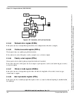


Chapter 2 Port Integration Module (S12XEP100PIMV1)
MC9S12XE-Family Reference Manual , Rev. 1.19
176
Freescale Semiconductor
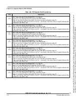
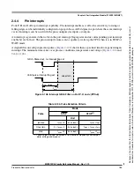
NOTE
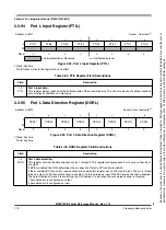
Due to internal synchronization circuits, it can take up to 2 bus clock cycles
until the correct value is read on PTF or PTIF registers, when changing the
DDRF register.
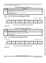
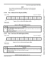
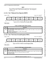
2.3.104 Port F Reduced Drive Register (RDRF)
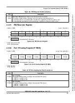
2.3.105 Port F Pull Device Enable Register (PERF)
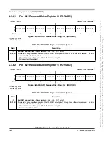
Address 0x037B
Access: User read/write
(1)
1. Read: Anytime.
Write: Anytime.
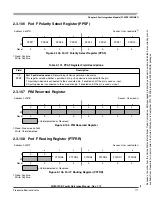
7
6
5
4
3
2
1
0
R
RDRF7
RDRF6
RDRF5
RDRF4
RDRF3
RDRF2
RDRF1
RDRF0
W
Reset
0
0
0
0
0
0
0
0
Figure 2-102. Port F Reduced Drive Register (RDRF)
Table 2-99. RDRF Register Field Descriptions
Field
Description
7-0
RDRF
Port F reduced drive
—Select reduced drive for outputs
This register configures the drive strength of output pins 7 through 0 as either full or reduced. If a pin is used as input
this bit has no effect.
1 Reduced drive selected (approx. 1/5 of the full drive strength).
0 Full drive strength enabled.
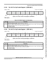
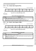
Address 0x037C
Access: User read/write
(1)
1. Read: Anytime.
Write: Anytime.
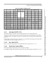
7
6
5
4
3
2
1
0
R
PERF7
PERF6
PERF5
PERF4
PERF3
PERF2
PERF1
PERF0
W
Reset
1
1
1
1
1
1
1
1
Figure 2-103. Port F Pull Device Enable Register (PERF)
Table 2-100. PERF Register Field Descriptions
Field
Description
7-0
PERF
Port F pull device enable
—Enable pull devices on input pins
These bits configure whether a pull device is activated, if the associated pin is used as an input. This bit has no effect
if the pin is used as an output. Out of reset all pull devices are enabled.
1 Pull device enabled.
0 Pull device disabled.
Because
of
an
order
from
the
United
States
International
Trade
Commission,
BGA-packaged
product
lines
and
part
numbers
indicated
here
currently
are
not
available
from
Freescale
for
import
or
sale
in
the
United
States
prior
to
September
2010:
S12XE
products
in
208
MAPBGA
packages


