


Chapter 14 Enhanced Capture Timer (ECT16B8CV3)
MC9S12XE-Family Reference Manual , Rev. 1.19
538
Freescale Semiconductor
14.3.2.9
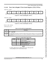
Timer Control Register 3/Timer Control Register 4 (TCTL3/TCTL4)
Read or write: Anytime
All bits reset to zero.
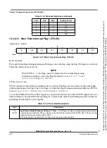
14.3.2.10 Timer Interrupt Enable Register (TIE)
Module Base + 0x000A
7
6
5
4
3
2
1
0
R
EDG7B
EDG7A
EDG6B
EDG6A
EDG5B
EDG5A
EDG4B
EDG4A
W
Reset
0
0
0
0
0
0
0
0
Figure 14-13. Timer Control Register 3 (TCTL3)
Module Base + 0x000B
7
6
5
4
3
2
1
0
R
EDG3B
EDG3A
EDG2B
EDG2A
EDG1B
EDG1A
EDG0B
EDG0A
W
Reset
0
0
0
0
0
0
0
0
Figure 14-14. Timer Control Register 4 (TCTL4)
Table 14-11. TCTL3/TCTL4 Field Descriptions
Field
Description
EDG[7:0]B
7, 5, 3, 1
Input Capture Edge Control
— These eight pairs of control bits configure the input capture edge detector
circuits for each input capture channel. The four pairs of control bits in TCTL4 also configure the input capture
edge control for the four 8-bit pulse accumulators PAC0–PAC3.EDG0B and EDG0A in TCTL4 also determine the
active edge for the 16-bit pulse accumulator PACB. See
EDG[7:0]A
6, 4, 2, 0
Table 14-12. Edge Detector Circuit Configuration
EDGxB
EDGxA
Configuration
0
0
Capture disabled
0
1
Capture on rising edges only
1
0
Capture on falling edges only
1
1
Capture on any edge (rising or falling)
Module Base + 0x000C
7
6
5
4
3
2
1
0
R
C7I
C6I
C5I
C4I
C3I
C2I
C1I
C0I
W
Reset
0
0
0
0
0
0
0
0
Figure 14-15. Timer Interrupt Enable Register (TIE)
Because
of
an
order
from
the
United
States
International
Trade
Commission,
BGA-packaged
product
lines
and
part
numbers
indicated
here
currently
are
not
available
from
Freescale
for
import
or
sale
in
the
United
States
prior
to
September
2010:
S12XE
products
in
208
MAPBGA
packages


