


Chapter 7 Background Debug Module (S12XBDMV2)
MC9S12XE-Family Reference Manual , Rev. 1.19
290
Freescale Semiconductor
For devices with external bus:
The following cycle count information is only valid when the external wait
function is not used (see wait bit of EBI sub-block). During an external wait
the BDM can not steal a cycle. Hence be careful with the external wait
function if the BDM serial interface is much faster than the bus, because of
the BDM soft-reset after time-out (see
).
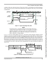
For hardware data read commands, the external host must wait at least 150 bus clock cycles after sending
the address before attempting to obtain the read data. This is to be certain that valid data is available in the
BDM shift register, ready to be shifted out. For hardware write commands, the external host must wait
150 bus clock cycles after sending the data to be written before attempting to send a new command. This
is to avoid disturbing the BDM shift register before the write has been completed. The 150 bus clock cycle
delay in both cases includes the maximum 128 cycle delay that can be incurred as the BDM waits for a
free cycle before stealing a cycle.
For firmware read commands, the external host should wait at least 48 bus clock cycles after sending the
command opcode and before attempting to obtain the read data. This includes the potential of extra cycles
when the access is external and stretched (+1 to m7 cycles) or to registers of the PRU (port
replacement unit) in emulation modes (if modes available). The 48 cycle wait allows enough time for the
requested data to be made available in the BDM shift register, ready to be shifted out.
NOTE
This timing has increased from previous BDM modules due to the new
capability in which the BDM serial interface can potentially run faster than
the bus. On previous BDM modules this extra time could be hidden within
the serial time.
For firmware write commands, the external host must wait 36 bus clock cycles after sending the data to be
written before attempting to send a new command. This is to avoid disturbing the BDM shift register
before the write has been completed.
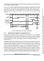
The external host should wait at least for 76 bus clock cycles after a TRACE1 or GO command before
starting any new serial command. This is to allow the CPU to exit gracefully from the standard BDM
firmware lookup table and resume execution of the user code. Disturbing the BDM shift register
prematurely may adversely affect the exit from the standard BDM firmware lookup table.
NOTE
If the bus rate of the target processor is unknown or could be changing or the
external wait function is used, it is recommended that the ACK
(acknowledge function) is used to indicate when an operation is complete.
When using ACK, the delay times are automated.
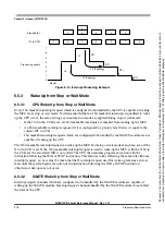
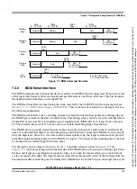
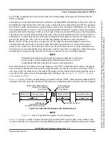
represents the BDM command structure. The command blocks illustrate a series of eight bit
times starting with a falling edge. The bar across the top of the blocks indicates that the BKGD line idles
in the high state. The time for an 8-bit command is 8
×
16 target clock cycles.
1
1. Target clock cycles are cycles measured using the target MCU’s serial clock rate. See
Section 7.4.6, “BDM Serial Interface”
and
Section 7.3.2.1, “BDM Status Register (BDMSTS)”
for information on how serial clock rate is selected.
Because
of
an
order
from
the
United
States
International
Trade
Commission,
BGA-packaged
product
lines
and
part
numbers
indicated
here
currently
are
not
available
from
Freescale
for
import
or
sale
in
the
United
States
prior
to
September
2010:
S12XE
products
in
208
MAPBGA
packages


