


Chapter 2 Port Integration Module (S12XEP100PIMV1)
MC9S12XE-Family Reference Manual , Rev. 1.19
Freescale Semiconductor
111
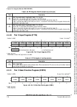
2.3.8
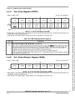
Port D Data Register (PORTD)
2.3.9
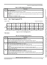
Port C Data Direction Register (DDRC)
Address 0x0005 (PRR)
Access: User read/write
(1)
1. Read: Anytime. In emulation modes, read operations will return the data from the external bus, in all other modes the data source
is depending on the data direction value.
Write: Anytime. In emulation modes, write operations will also be directed to the external bus.
7
6
5
4
3
2
1
0
R
PD7
PD6
PD5
PD4
PD3
PD2
PD1
PD0
W
Altern.
Function
DATA7
DATA6
DATA5
DATA4
DATA3
DATA2
DATA1
DATA0
Reset
0
0
0
0
0
0
0
0
Figure 2-6. Port D Data Register (PORTD)
Table 2-9. PORTD Register Field Descriptions
Field
Description
7-0
PD
Port D general purpose input/output data
—Data Register
Port D pins 7 through 0 are associated with data I/O lines DATA[7:0] respectively in expanded modes.
When not used with the alternative function, these pins can be used as general purpose I/O.
If the associated data direction bits of these pins are set to 1, a read returns the value of the port register, otherwise
the buffered pin input state is read.
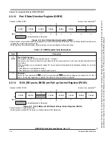
Address 0x0006 (PRR)
Access: User read/write
(1)
1. Read: Anytime. In emulation modes, read operations will return the data from the external bus, in all other modes the data source
is depending on the data direction value.
Write: Anytime. In emulation modes, write operations will also be directed to the external bus.
7
6
5
4
3
2
1
0
R
DDRC7
DDRC6
DDRC5
DDRC4
DDRC3
DDRC2
DDRC1
DDRC0
W
Reset
0
0
0
0
0
0
0
0
Figure 2-7. Port C Data Direction Register (DDRC)
Because
of
an
order
from
the
United
States
International
Trade
Commission,
BGA-packaged
product
lines
and
part
numbers
indicated
here
currently
are
not
available
from
Freescale
for
import
or
sale
in
the
United
States
prior
to
September
2010:
S12XE
products
in
208
MAPBGA
packages


