


Appendix A Electrical Characteristics
MC9S12XE-Family Reference Manual Rev. 1.19
Freescale Semiconductor
1247
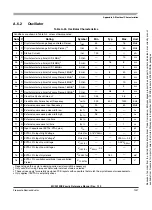
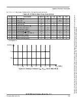
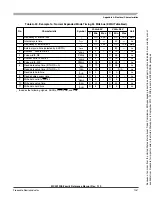
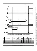
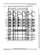
Table A-30. Example 1a: Normal Expanded Mode Timing 50 MHz bus (EWAIT disabled)
No.
Characteristic
Symbol
V
DD5
=5.0V
V
DD5
=3.3V
Unit
C
Min
Max
C
Min
Max
-
Frequency of internal bus
f
i
-
D.C.
50.0
-
D.C.
25.0
MHz
-
Internal cycle time
t
cyc
-
20
∞
-
40
∞
ns
-
Frequency of external bus
f
o
-
D.C.
25.0
-
D.C.
12.5
MHz
1
External cycle time (selected by EXSTR)
t
cyce
-
40
∞
-
80
∞
ns
2
Address
1
valid to RE fall
1
Includes the following signals: ADDRx, UDS, LDS, and CSx.
t
ADRE
D
4
-
D
13
-
ns
3
Pulse width, RE
PW
RE
D
28
-
D
58
-
ns
4
Address valid to WE fall
t
ADWE
D
4
-
D
15
-
ns
5
Pulse width, WE
PW
WE
D
18
-
D
38
-
ns
6
Read data setup time (if ITHRS = 0)
t
DSR
D
19
-
D
38
-
ns
Read data setup time (if ITHRS = 1)
t
DSR
D
23
-
D
N/A
ns
7
Read data hold time
t
DHR
D
0
-
D
0
-
ns
8
Read enable access time
t
ACCR
D
4
-
D
4
-
ns
9
Write data valid to WE fall
t
WDWE
D
5
-
D
5
-
ns
10
Write data setup time
t
DSW
D
23
-
D
43
-
ns
11
Write data hold time
t
DHW
D
6
-
D
4
-
ns
Because
of
an
order
from
the
United
States
International
Trade
Commission,
BGA-packaged
product
lines
and
part
numbers
indicated
here
currently
are
not
available
from
Freescale
for
import
or
sale
in
the
United
States
prior
to
September
2010:
S12XE
products
in
208
MAPBGA
packages


