VI-12
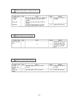
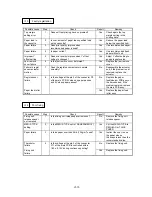
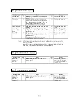
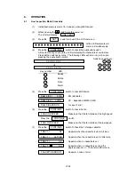
M-4 Malfunction of control panel switches
Possible cause
Step
Check
Result
Remedy
Mis-operation
1
Are the switches operated according to the
operation manual?
No
Operate the switches
correctly following the
operation manual.
Switch
2
When a switch is pressed, does the voltage of
the following signals change from 5V to 0V?
Yes
Replace the Main PCB
assy.
Control panel
PCB
Switch flat cable
Main PCB
No
Replace the control panel
unit or the switch flat
cable.
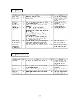
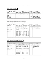
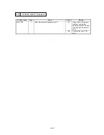
M-5 "12 COVER OPEN " is displayed even if the upper cover is closed
Possible cause
Step
Check
Result
Remedy
Upper cover
1
Does the upper cover hook press the actuator
of the interlock switch on the main PCB
No
Replace the upper cover
assy.
Main PCB
correctly when upper cover is closed?
Yes
Replace the main PCB
assy.
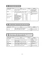
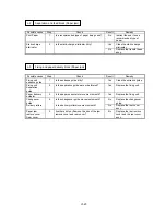
M-6 "CHECK XX TRAY" is displayed even if a paper-loaded cassette is mounted
(or even if a paper is set on MP tray) XX is MP/T1/T2
Possible cause
Step
Check
Result
Remedy
Mis-operation
1
Is the paper feed mode set correctly?
No
Set paper feed mode
correctly.
Actuator
2
Does the actuator for the paper empty sensor
operate smoothly?
No
Reassemble or replace
the actuator.
Paper empty
sensor
Feed flat cable
3
Does the voltage of P5-3 (or P5-14) in the
Paper feeder PCB connector rise from 0V to
5V when the paper empty sensor is covered?
No
Replace the paper
feed/size-sw PCB assy or
feed flat cable.
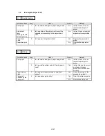
Paper feed flat
cable
4
Does the voltage of P3-3 (or P3-14) in the
main PCB connector rise from 0V to 5V when
No
Replace the feed flat
cable.
Main PCB
the paper empty sensor is covered?
Yes
Replace the main PCB
assy.
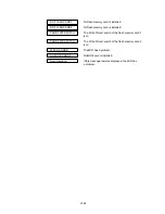
Panel PCB
−
P1-7
−
P1-19
−
P1-9
−
P1-5
−
P1-15
−
P1-17
−
P1-13
−
P1-11
Main PCB
P1-7
P1-19
P1-9
P1-5
P1-15
P1-17
P1-13
P1-11
Signal
SW8(SEL)
SW7(MODE/EMULATION)
SW6(FONT/ECONOMY)
SW5(FORM FEED/FEEDER)
SW4(SET/COPY)
SW3(CONTINUE/SHIFT)
SW2(DOWN/RESET)
SW1(UP/TEST)
Содержание HL-2060
Страница 1: ...MECHANICS ELECTRONICS SERVICE MANUAL LASER PRINTER ...
Страница 41: ...III 8 A B F C D E 1 E 2 E 3 E 4 E 5 F Figure 3 7 Paper Feed Size SW PCB Circuit ...
Страница 129: ...VII 16 Test for memory MEMORY DISPLAY MEMORY DEBUG MEMORY TEST exit MENU ...
Страница 136: ...Appendix A 2 Paper Feed Size SW PCB Circuitry Diagram 1 1 CODE UK4067000 B512011 012 CIR NAME A 2 ...
Страница 137: ...Appendix A 3 Main PCB Circuitry Diagram 1 7 CODE UK4058000 B512006 CIR 1 7 NAME A 3 ...
Страница 138: ...Appendix A 4 Main PCB Circuitry Diagram 2 7 CODE UK4058000 B512006 CIR 2 7 NAME A 4 ...
Страница 139: ...Appendix A 5 Main PCB Circuitry Diagram 3 7 CODE UK4058000 B512006 CIR 3 7 NAME A 5 ...
Страница 140: ...Appendix A 6 Main PCB Circuitry Diagram 4 7 CODE UK4058000 B512006 CIR 4 7 NAME A 6 ...
Страница 141: ...Appendix A 7 Main PCB Circuitry Diagram 5 7 CODE UK4058000 B512006 CIR 5 7 NAME A 7 ...
Страница 142: ...Appendix A 8 Main PCB Circuitry Diagram 6 7 CODE UK4058000 B512006 CIR 6 7 NAME A 8 ...
Страница 143: ...Appendix A 9 Main PCB Circuitry Diagram 7 7 CODE UK4058000 B512006 CIR 7 7 NAME A 9 ...
Страница 144: ...Appendix A 10 Control Panel PCB Circuitry Diagram 1 1 CODE UK4077000 B512005 CIR NAME A 10 ...
Страница 145: ...Appendix A 11 Laser LD PCB Circuitry Diagram 1 1 CODE UK3253000 B48K253 CIR NAME A 11 ...
Страница 147: ...June 98 54T046NE0 HL2060 ...


