VI-6
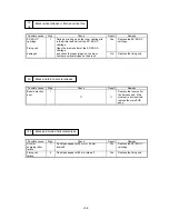
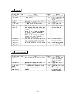
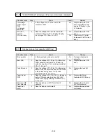
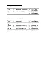
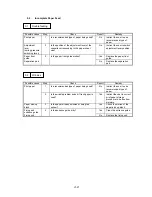
I-3 Completely blank
Possible cause
Step
Check
Result
Remedy
EP-ED HC
cartridge
1
Does printed image improve when the EP-ED
HC
cartridge is replaced?
Yes
Replace the EP-ED HC
cartridge.
Development
input signal
error
2
Do the pins 3, 4 and 5 of the connector?
P6 on the main PCB have the following value
respectively when a sheet of paper is fed from
the MP tray?
P6-3 pin (DBAC) --- Change in voltage from
6V approx. to 0V just when a sheet of paper is
fed from the registration unit.
P6-4 pin (DBDC) --- Change in voltage from
9V approx. to 0V just when a sheet of paper is
fed from the registration unit.
P6-5 pin (DNSTY) --- Change in voltage to
2.5V just when a sheet of paper is fed.
No
Replace the main PCB
assy or the harness.
Failure in power
supply terminal
3
Is there any dirt on the cartridge side
development terminal of the transfer unit and
on the terminal of the high-voltage power
supply development unit? (is there continuity
between them?)
No
Clean the terminal to
assure the continuity.
LD failure
4
Does print quality improve when the laser
unit is improved?
Yes
Replace the laser unit or
the harness.
Failure in
development
high-voltage
circuit
No
Replace the high-voltage
power supply PCB assy.
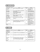
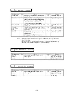
I-4 All black
Possible cause
Step
Check
Result
Remedy
Beam detection
error
1
Is the printer hung up with the PRINT message
remaining on the display even after a printing
when only a copy is printed?
Yes
Replace the laser unit or
the harness.
EP-ED HC
cartridge
2
Does printed image improve when the EP-ED
HC
cartridge is replaced?
Yes
Replace the EP-ED HC
cartridge.
Charging input
signal error
3
Do the pins 1 and 2 of the connector P6 on the
main PCB have the following value
respectively when a sheet of paper is fed from
the MP tray?
P6-1 pin (HV1AC) --- Change in voltage from
6V approx. to 0V just when a sheet of paper is fed.
P6-2 pin (HV1DC) --- Change in voltage from
9V approx. to 0V just when a sheet of paper is fed.
No
Replace the main PCB
assy or the harness.
Dirt on power
supply terminal
4
Is there any dirt on the cartridge side charging
terminal of the transfer unit and on the terminal
of the high-voltage power supply charging unit?
No
Clean the contact to
assure the continuity.
Failure in the
charging high-
voltage circuit
LD failure
(is there continuity between them?)
Yes
Replace the high-voltage
power supply PCB assy
and, if the problem is not
resolved, replace the laser
unit or the harness.
Содержание HL-2060
Страница 1: ...MECHANICS ELECTRONICS SERVICE MANUAL LASER PRINTER ...
Страница 41: ...III 8 A B F C D E 1 E 2 E 3 E 4 E 5 F Figure 3 7 Paper Feed Size SW PCB Circuit ...
Страница 129: ...VII 16 Test for memory MEMORY DISPLAY MEMORY DEBUG MEMORY TEST exit MENU ...
Страница 136: ...Appendix A 2 Paper Feed Size SW PCB Circuitry Diagram 1 1 CODE UK4067000 B512011 012 CIR NAME A 2 ...
Страница 137: ...Appendix A 3 Main PCB Circuitry Diagram 1 7 CODE UK4058000 B512006 CIR 1 7 NAME A 3 ...
Страница 138: ...Appendix A 4 Main PCB Circuitry Diagram 2 7 CODE UK4058000 B512006 CIR 2 7 NAME A 4 ...
Страница 139: ...Appendix A 5 Main PCB Circuitry Diagram 3 7 CODE UK4058000 B512006 CIR 3 7 NAME A 5 ...
Страница 140: ...Appendix A 6 Main PCB Circuitry Diagram 4 7 CODE UK4058000 B512006 CIR 4 7 NAME A 6 ...
Страница 141: ...Appendix A 7 Main PCB Circuitry Diagram 5 7 CODE UK4058000 B512006 CIR 5 7 NAME A 7 ...
Страница 142: ...Appendix A 8 Main PCB Circuitry Diagram 6 7 CODE UK4058000 B512006 CIR 6 7 NAME A 8 ...
Страница 143: ...Appendix A 9 Main PCB Circuitry Diagram 7 7 CODE UK4058000 B512006 CIR 7 7 NAME A 9 ...
Страница 144: ...Appendix A 10 Control Panel PCB Circuitry Diagram 1 1 CODE UK4077000 B512005 CIR NAME A 10 ...
Страница 145: ...Appendix A 11 Laser LD PCB Circuitry Diagram 1 1 CODE UK3253000 B48K253 CIR NAME A 11 ...
Страница 147: ...June 98 54T046NE0 HL2060 ...


