II-7
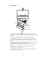
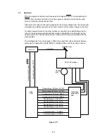
Step 1 Primary charge
,,,
,,,
,,
,,,,
,,,,
,,
,,,
,,,
,
,,
,,,
,
,,
,,
,,
,,
,,,
,,
,,,
,,,
,
,,
,,,
,,,
,,,
,
,,,
,,,
,,
,,
,,
,,
,,
,,
,,
,,
,,
,,
,
,,,
,
,
,,,
,,,
,
,,
,,,,
,,,,
,,
,,,
,,,
Figure 2.9
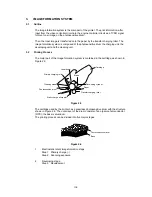
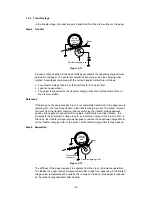
As preparation for latent image formation, a uniform negative potential is applied to the
photosensitive drum surface. The printer uses the charging method that directly charges
the drum for the primary charge.
The primary charging roller consists of conductive rubber. In addition to DC bias, AC bias
is applied to the primary charging roller to keep the potential on the drum surface uniform.
This DC bias is changed with the developing DC bias.
This charging method has advantages such as lower applied voltage, less ozone
generation, etc., compared with the corona charge system.
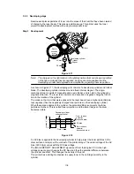
Step 2 Scanning exposure
+
+
+
_
_
_
Figure 2.10
When the laser beam scans the drum surface, it causes the charge to be neutralized in
the areas struck by the beam. Areas on the drum with no charge form the electrostatic
latent image.
Laser beam
Unexposed area
Exposed area
DC bias
AC bias
Photosensitive drum
Primary charging roller
Содержание HL-2060
Страница 1: ...MECHANICS ELECTRONICS SERVICE MANUAL LASER PRINTER ...
Страница 41: ...III 8 A B F C D E 1 E 2 E 3 E 4 E 5 F Figure 3 7 Paper Feed Size SW PCB Circuit ...
Страница 129: ...VII 16 Test for memory MEMORY DISPLAY MEMORY DEBUG MEMORY TEST exit MENU ...
Страница 136: ...Appendix A 2 Paper Feed Size SW PCB Circuitry Diagram 1 1 CODE UK4067000 B512011 012 CIR NAME A 2 ...
Страница 137: ...Appendix A 3 Main PCB Circuitry Diagram 1 7 CODE UK4058000 B512006 CIR 1 7 NAME A 3 ...
Страница 138: ...Appendix A 4 Main PCB Circuitry Diagram 2 7 CODE UK4058000 B512006 CIR 2 7 NAME A 4 ...
Страница 139: ...Appendix A 5 Main PCB Circuitry Diagram 3 7 CODE UK4058000 B512006 CIR 3 7 NAME A 5 ...
Страница 140: ...Appendix A 6 Main PCB Circuitry Diagram 4 7 CODE UK4058000 B512006 CIR 4 7 NAME A 6 ...
Страница 141: ...Appendix A 7 Main PCB Circuitry Diagram 5 7 CODE UK4058000 B512006 CIR 5 7 NAME A 7 ...
Страница 142: ...Appendix A 8 Main PCB Circuitry Diagram 6 7 CODE UK4058000 B512006 CIR 6 7 NAME A 8 ...
Страница 143: ...Appendix A 9 Main PCB Circuitry Diagram 7 7 CODE UK4058000 B512006 CIR 7 7 NAME A 9 ...
Страница 144: ...Appendix A 10 Control Panel PCB Circuitry Diagram 1 1 CODE UK4077000 B512005 CIR NAME A 10 ...
Страница 145: ...Appendix A 11 Laser LD PCB Circuitry Diagram 1 1 CODE UK3253000 B48K253 CIR NAME A 11 ...
Страница 147: ...June 98 54T046NE0 HL2060 ...

