Debug Support
8-14
Copyright © ARM Limited 2000. All rights reserved.
8.4.3
Scan chain 3
This scan chain allows ARM946E-S to control an optional external boundary scan
chain. You can determine the length of scan chain 3.
8.4.4
Scan chain 15
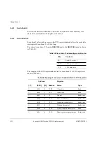
Scan chain 15 allows debug access to the CP15 register bank and allows the cache to be
interrogated. Scan chain 15 is 39 bits long.
The order of scan chain 15 from the DBGTDI input to the DBGTDO output is shown
in Table 8-4.
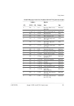
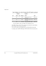
The mapping of the CP15 register address field of scan chain 15 to CP15 registers is
shown in Table 8-5.
Table 8-4 Scan chain 15 addressing mode bit order
Bits
Contents
38
Read = 0, write = 1
37:32
CP15 register address
31:0
CP15 data value
Table 8-5 Mapping of scan chain 15 address field to CP15 registers
Address
Register
[37]
[36:33]
[32]
Number
Name
Type
0
0000
0
C0.ID
ID register
Read
0
0000
1
C0.C
Cache type
Read
0
0001
0
C1
Control
Read/write
0
0010
0
C2.D
Data cachable bits
Read/write
0
0010
1
C2.I
Instruction cachable bits
Read/write
0
0011
0
C3
Write buffer control
Read/write
0
0100
0
C0.M
Tightly-coupled memory size
Read
0
0101
0
C5.D
Data space access permissions
Read/write
Содержание ARM946E-S
Страница 1: ...ARM DDI 0155A ARM946E S Technical Reference Manual ...
Страница 6: ...vi Copyright ARM Limited 2000 All rights reserved ARM DDI 0155A 04 Limited Confidential ...
Страница 54: ...Programmer s Model 2 34 Copyright ARM Limited 2000 All rights reserved ARM DDI 0155A ...
Страница 70: ...Caches 3 16 Copyright ARM Limited 2000 All rights reserved ARM DDI 0155A ...
Страница 78: ...Protection Unit 4 8 Copyright ARM Limited 2000 All rights reserved ARM DDI 0155A ...
Страница 98: ...Bus Interface Unit and Write Buffer 6 14 Copyright ARM Limited 2000 All rights reserved ARM DDI 0155A ...
Страница 112: ...Coprocessor Interface 7 14 Copyright ARM Limited 2000 All rights reserved ARM DDI 0155A ...


